Ac undershoot, maximum overshoot area above vddq, Vid(ac), ac differential input voltage, Vix(ac), ac differential input cross point voltage – Teledyne LeCroy QPHY-DDR2 User Manual
Page 39: Read bursts (outputs), Sout (output slew rate), Soutr and soutf, Tslmr, Qphy-ddr2 software option
QPHY-DDR2 Software Option
QPHY-DDR2-OM-E Rev
A
39
AC Undershoot, Maximum overshoot area above VDDQ
Prerequisite: AC Undershoot maximum peak amplitude, needed to compute area.
Maximum undershoot area below VSSQ.
Note: The maximum requirements for peak amplitude were reduced from 0.9V to 0.5V. Register vendor data sheets specify the maximum
over/undershoot induced in specific RDIMM applications. DRAM vendor data sheets also specify the maximum overshoot/undershoot that
their DRAM can tolerate. This allows the RDIMM supplier to understand whether the DRAM can tolerate the overshoot that the register
induces in the specific RDIMM application. A variable allows this limit to be changed.
Tests Requiring Single Ended Probing of Differential Signal
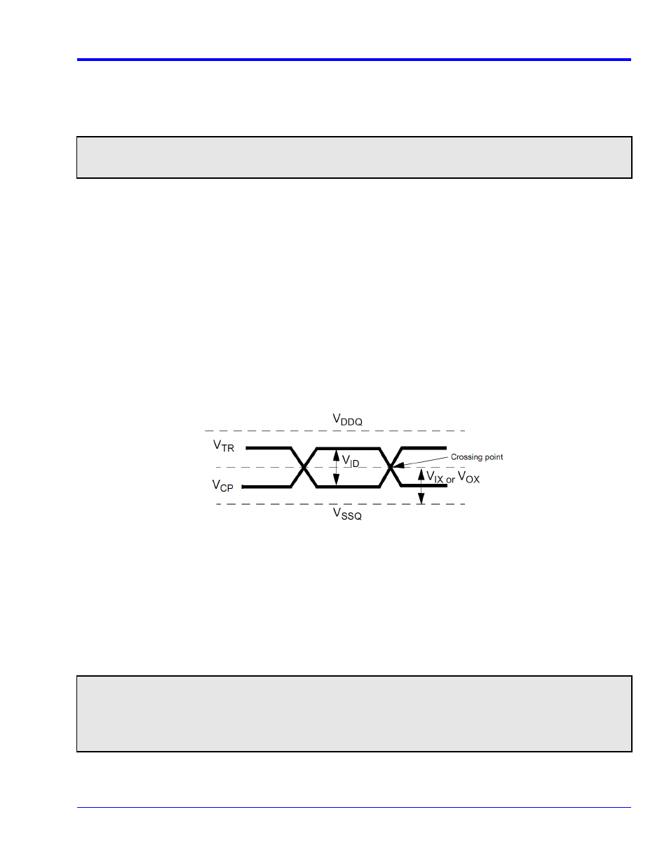
VID(ac), AC Differential Input Voltage
VID(ac) specifies the input differential voltage | VTR - VCP | required for switching, where VTR is the true input
signal (such as CK, DQS, LDQS or UDQS) and VCP is the complementary input signal (such as CK, DQS, LDQS
or UDQS). The minimum value is equal to VIH(ac) - VIL(ac). This test requires probing each half of a differential
signal. This is only available in the configurations using 4 probes.
VIX(ac), AC Differential Input Cross Point Voltage
The typical value of VIX(ac) is expected to be about 0.5 x VDDQ of the transmitting device and VIX(ac) is
expected to track variations in VDDQ. VIX(ac) indicates the voltage at which differential input signals must cross.
This test requires probing each half of a differential signal. This is only available in the configurations using 4
probes.
Figure 22. Differential signal levels [JESD79-2E figure 74]
Read B
ursts
(Outputs)
Sout (Output Slew Rate)
SoutR and SoutF
Apply to all output signals (DQn data signals), but only for 400, 533 and 667 MHz device, not for 800 MHz device.
The output slew rate is measured from VIL(ac) to VIH(ac) for the rising edge and from VIH(ac) to VIL(ac) for the
falling edge. DRAM output slew rate specification applies to 400, 533 & 667 MHz speed devices.
PLEASE NOTE THE FOLLOWING:
Absolute value of the slew rate as measured from (dc) to (dc) >= Slew rate as measured from (ac) to (ac).This is guaranteed by design
and characterization.
Output slew rate for falling and rising edges is measured between VTT - 250 mV and VTT + 250 mV for single ended signals. For
differential signals (e.g. DQS - DQS#) output slew rate is measured between DQS - DQS# = - 500 mV and DQS - DQS# = + 500 mV.
Output slew rate is guaranteed by design, but is not necessarily tested on each device.
tSLMR
This is the ratio of the rising edge slewrate to the falling edge slewrate. This is a test recommended by Intel but