Communication Concepts AN779 Application Note User Manual
Page 7
AR
C
HIVE INF
O
RMA
TI
O
N
PRODUCT TRANSFERRED T
O
M/A
–
COM
AN779
7
RF Application Reports
The amount of negative feedback is difficult to determine,
as it depends on the device type and size and the physical
circuit layout. The operating voltage has a minimal effect on
the transistor input characteristics, which are more
determined by the electrical size of the die. High-power
transistors have lower input impedances and higher
capacitances, and phase errors are more likely to occur due
to circuit inductances.
Since the input capacitance is an indication of electrical
size of the device, we can take the paralleled value (X
p
) at
2 MHz, which is X
s
+ (R
s
2
/X
s
) and for MRF433 3.5 +
(9.1
2
/3.5) = 27 ohms. The X
p
of the largest devices available
today is around 10 ohms at 30 MHz, and experience has
shown that the maximum feedback should be limited to about
5 dB in such case. Using these figures as constants, and
assuming the G
PE
is at least 10 dB, we can estimate the
amount of feedback as: 5/(10
2
/27) + 5 = 6.35 dB, although
only 4 dB was necessary in this design due to the low
∆G
PE
of the devices.
The series base resistors (R4 and R5) can be calculated
for 4 dB loss as follows:
I
in
[(V
in
x
∆4 dB) – V
in
]
=
0.04
[(0.79 x 1.58) – 0.79]
= 11.45 ohms, or
11.45/2 = 5.72 ohms each.
Z
in
(2 MHz) = (9.1
2
+ 3.5
2
) = 9.75 ohms,
in Class AB push-pull 19.5 ohms.
P
in
= 20 W – 28 dB = 20/630 = 0.032 W
V
RMS
(base to base) =
√(0.032 x 19.5) = 0.79 V
I
in
= V
in
/R
in
= 0.79/19.5 = 0.04 A
∆V4 db = [Log
–1
(4/10)] = 1.58 V
The parallel capacitors (C3 and C4) should be selected
to resonate with R (5.7 ohms) somewhere in the midband.
At 15 MHz, out of the standard values, 1800 pF appears
to be the closest, having a negligible reactance at 2 MHz,
and 2.8 ohms at 30 MHz, where most of the capacitive
reactance is canceled by the transformer winding induc-
tance.
X
X
X
X
X
X
X
X X
X
X
X
X
X
X
X
X
X
X
X
X
X
X
X
X
X
X
X
X
X
X
X
X
X
X
X
X
X
X
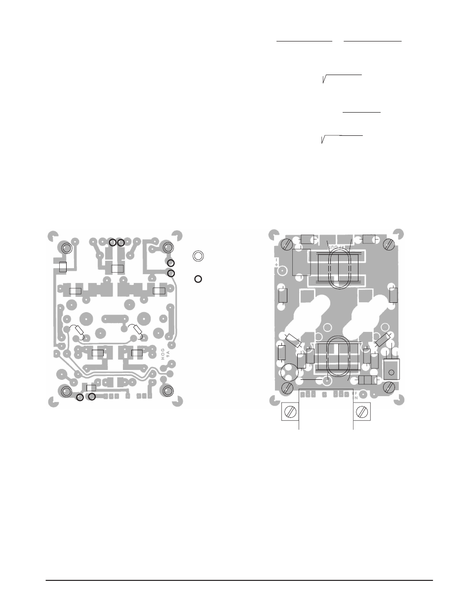
= Feedthrough Eyelets
= Terminal Pins
= Board Standoffs
C8
L4
L1
L6
L7
T2
C
C
E
Q2
E
Q3
E
E
T2
B
B
R7
Q1
L3
R5
L5
R3
R1
R2
R6
H1
L2
C7
C2
C6
C5
D2
D1
C4
C3
C1
Figure 9. Component Layout Diagram of 20 W, 55 dB High-Performance Drive
The leads of D1 and D2 are bent to allow the diodes to
contact the transistor mounting flanges.
Note: The mounting pad of Q1 must be connected to the
lower side of the board through an eyelet or a plated
through-hole.