Communication Concepts AN779 Application Note User Manual
Page 3
AR
C
HIVE INF
O
RMA
TI
O
N
PRODUCT TRANSFERRED T
O
M/A
–
COM
AN779
3
RF Application Reports
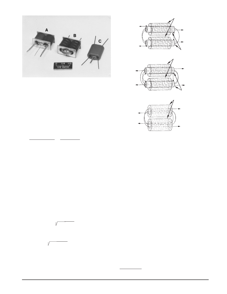
Figure 3. Examples of broadband transformers.
Variations of these are used in all designs of this article
(see text). All ferrites in transformers are Fair-Rite
Products Corp. #2643006301 ferrite beads.*
and impedance levels are relatively high. Problems were en-
countered especially with the output transformer design,
where an inductance of 4
µH minimum is required in the one-
turn winding across the collectors, when the load impedance
is
20
2 (13.6 – 2.5)
2
= 12.3 ohms.
4,8
=
P
out
2 (V
CE
– V
CEsat
)
2
Ferrites having sufficiently low-loss factors at 30 MHz
range only up to 800 – 1000 in permeability and the
inductance is limited to 2.5 – 3.0
µH in the physical size
required. This would also limit the operation to approximately
4 MHz, below which excessive harmonics are generated and
the efficiency will degrade. One possible solution is to
increase the number of turns, either by using the metal tubes
for only part of the windings as in Figure 4B, or simply by
winding the two sets of windings randomly through ferrite
sleeves or a series of beads (Figures 3C and 4C). In the
latter, the metal tubes can be disregarded or can be used
only for mounting purposes. T3 was eventually replaced with
a transformer of this type, although not shown in Figure 1.
Below approximately 100 MHz, the input impedances of
devices of the size of MRF475 and smaller are usually
capacitive in reactance, and the X
s
is much smaller than the
R
s
, (Low Q) For practical purposes, we can then use the
formula
(Rs
2
+ X
s
2
)
to find the actual input impedance of the device. The data-
sheet numbers for 30 MHz are 4.5, –j2.4 ohms, and we get
(4.5
2
+ 2.4
2
) = 5.1 ohms.
The base-to-base impedance in a push-pull circuit would be
four times the base-to-emitter impedance of one transistor.
However, in Class AB, where the base emitter junction is for-
ward biased and the conduction angle is increased, the im-
pedance becomes closer to twice that of one device. The
rounded number of 11 ohms must then be matched to the
Metal Tubings
Metal Tubings
Ferrite Sleeves
Ferrite Sleeves
Ferrite Sleeves
Lo Z
Hi Z
Hi Z
Hi Z
Lo Z
Lo Z
A
B
C
Figure 4. The turns ratios shown above are imaginary
and do not necessarily lead to correct design practices
driver output. The drive power required with the 10 dB speci-
fied minimum gain is
P
out
/Log
–1
(G
PE
/10) = 2.0 W
and the driver output impedance using the previous formula
is 2(11.1
2
)/2 = 123 ohms. The 11 ohms in series with the
gain-leveling networks (C8, R8 and C9, R11) is 17 ohms.
The closest practical transformer for this interface would be
one with 9:1 impedance ratio. This would present a higher-
than-calculated load impedance to the driver collectors, and
for the best linearity the output load should be lower than re-
quired for the optimum gain and efficiency. Considering that
the device input impedance increases at lower frequencies,
a better overall match is possible with a 4:1, especially since
the negative feedback is limited to only 4 dB at 2 MHz due to
its effect on the efficiency and linearity.
The maximum amount of feedback a circuit can tolerate
depends much on the physical layout, the parasitic
inductances, and impedance levels, since they determine the
phase errors in the loop. Thus, in general, the high-level
stages should operate with lower feedback than the low-level
stages.
The maximum amount of feedback the low-level driver
can tolerate without noticeable deterioration in IMD is about
12 dB. This makes the total 16 dB, but from the data sheets
we find that the combined gain variation for both devices
from 2 to 30 MHz is around 29 dB. The difference, or 13 dB,
should be handled by the gain–leveling networks.
*Wallkill, N.Y. 12589