Gate, trigger and timebase characteristics – Atec Agilent-53200A Series User Manual
Page 8
8
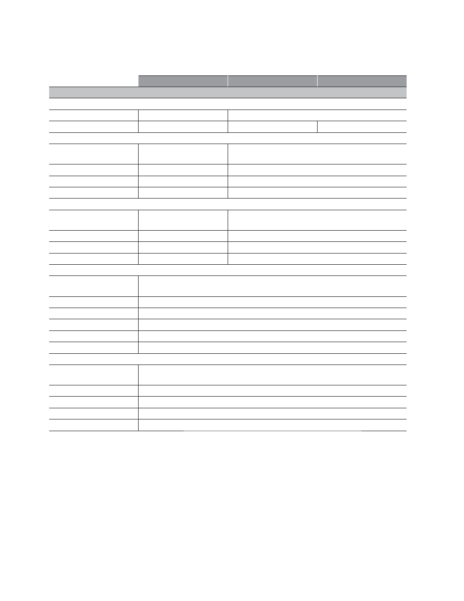
Gate, Trigger and Timebase Characteristics
53210A
53220A
53230A
Gate characteristics (nom)
Gate
Source
Time, external
Time, external or advanced
Gate time (step size)
1
1 ms - 1000 s (10 µs)
100 µs - 1000 s (10 µs)
1 µs - 1000 s (1 µs)
Advanced: gate start
Source
N/A
Internal or external, Ch 1/Ch 2
(unused standard channel input)
Slope
N/A
Positive or negative
Delay time
1
N/A
0 s to 10 s in 10 ns steps
Delay events (edges)
N/A
0 to 10
8
for signals up to 100 MHz
Advanced: gate stop hold-off
Source
N/A
Internal or external, Ch 1/Ch 2
(unused standard channel input)
Slope
N/A
Positive or negative
Hold-off time
1
N/A
Hold-off Time settable from 60 ns to 1000 s
Hold-off events (edges)
N/A
0 to 10
8
(minimum width (positive or negative) >60 ns)
External gate input characteristics (typ)
Connector
Rear panel BNC(f)
Selectable as external gate input or gate output signal
Impedance
1 kΩ when selected as external gate input
Level
TTL compatible
Slope
Selectable positive or negative
Gate to gate timing
3 µs gate end to next gate start
Damage level
<-5 V, >+10 V
Gate output characteristics (typ)
Connector
Rear panel BNC(f)
Selectable as external gate input or gate output signal
Impedance
50 Ω when selected for gate output
Level
TTL compatible
Slope
Selectable positive or negative
Damage level
<-5 V, >+10 V