Ap3595, Recommended operating conditions, Electrical characteristics – Diodes AP3595 User Manual
Page 5
AP3595
Document number: DS36749 Rev. 1 - 2
5 of 23
January 2014
© Diodes Incorporated
AP3595
A Product Line of
Diodes Incorporated
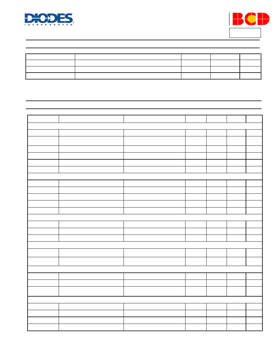
Recommended Operating Conditions
Symbol
Parameter
Min
Max
Unit
V
CC
Supply Input Voltage
10.8
13.2
V
T
A
Operating Ambient Temperature
-40
+85
°C
T
J
Operating Junction Temperature
-40
+125
°C
Electrical Characteristics
(@V
CC
=12V, T
A
=+25
C, unless otherwise specified.)
Symbol
Parameter
Conditions
Min
Typ
Max
Unit
SUPPLY INPUT
V
CC
Supply Input Voltage
–
10.8
–
13.2
V
I
CC
Supply Current
HG and LG Open, V
CC
=12V,
Switching
–
5
–
mA
I
Q
Quiescent Current
No Switching, I
PCC
=0mA
–
4
–
mA
V
PCC
Regulated Supply Voltage
RT/EN=0V, I
PCC
=0mA
8
9
10
V
V
RTH
POR Threshold
–
8
9
10
V
V
HYS
POR Hysteresis
–
–
1
–
V
CHIP ENABLE/FREQUENCY SETTING
I
RT/EN
RT/EN Sourcing Current
V
RT/EN
=GND
100
150
200
A
V
RT/EN
RT/EN Voltage
R
RT
=33kΩ
–
1
–
V
–
Switching Frequency Setting Range
–
50
–
1000
kHz
f
OSC
Free Run Switching Frequency
R
RT
=33kΩ
270
300
330
kHz
△ f
OSC
Switching Frequency Accuracy
f
OSC
=200kHz to 500kHz
-15
–
15
%
OSCILLATOR
–
Maximum Duty Cycle
–
–
40
–
%
–
Minimum Duty Cycle
–
–
0
–
%
V
OSC
Ramp Amplitude
V
CC
=12V
–
3.5
–
V
POWER SAVING MODE
V
PSI_H
Threshold Voltage for Entering Dual
Phase
V
PSI
rising
1.2
–
–
V
V
PSI_L
Threshold Voltage for Entering
Single Phase
V
PSI
falling
–
–
0.4
V
REFERENCE VOLTAGE
V
REF
Reference Voltage Accuracy
I
REF
=100
A
1.98
2.0
2.02
V
△ V
REF
Reference Voltage Load Regulation
I
REF
=0 to 2mA
-5
–
5
mV
△ V
FB
Output Voltage Accuracy
|V
REFIN
-V
FB
|, V
CC
=12V, No Load,
R
DRP
=0, V
REFIN
=0.8V to 1.6V
–
–
5
mV
ERROR AMPLIFIER
A
O
Open Loop DC Gain
Guaranteed by design
70
80
–
dB
G
BW
Gain Bandwidth Product
C
LOAD
=5pF, Guaranteed by design
–
20
–
MHz
SR
Slew Rate
Guaranteed by design
15
20
–
V/
s
I
COMP
Maximum Current (Sink and Source)
V
COMP
=1.6V
1.5
2.0
–
mA