Ap3595, Pin descriptions – Diodes AP3595 User Manual
Page 3
AP3595
Document number: DS36749 Rev. 1 - 2
3 of 23
January 2014
© Diodes Incorporated
AP3595
A Product Line of
Diodes Incorporated
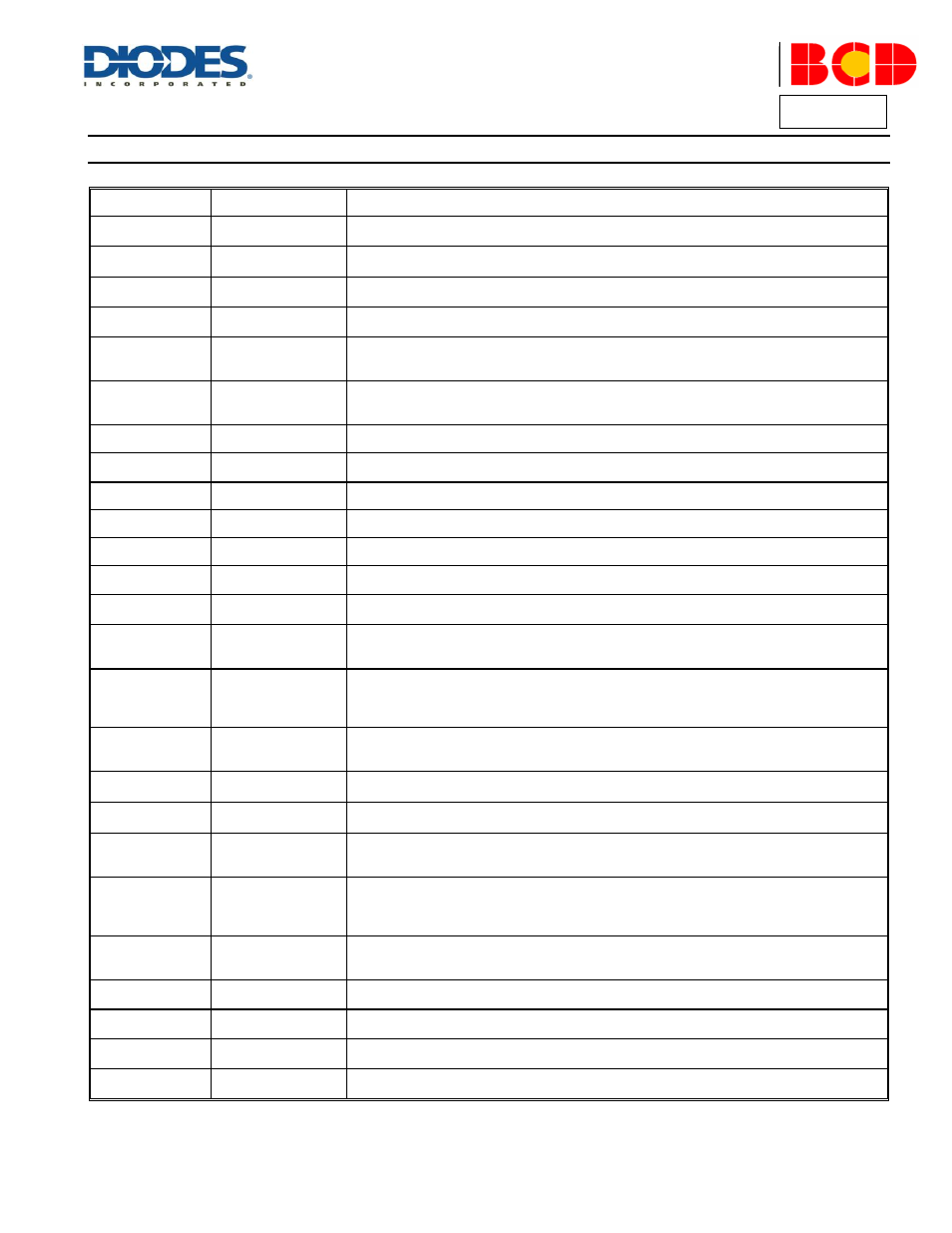
Pin Descriptions
Pin Number
Pin Name
Function
1
REFIN
External Reference Input. This is the input pin of external reference voltage. Connect a voltage
divider from VREF to REFIN and FBRTN to set the reference voltage
2
VREF
Output for Reference Voltage. This is the output pin of high precision 2V reference voltage.
Bypass this pin with a 1
F ceramic capacitor to FBRTN
3
RT/EN
Operation Frequency Setting. Connecting a resistor between this pin and GND to set the
operation frequency. Pull this pin to ground to shut down the AP3595
4
IOFS
Current Balance Adjustment. Connect a resistor from this pin to VREF or GND to adjust the
current sharing
5
COMP
Error Amplifier Output. This is the output of the error amplifier (EA) and the non-inverting input
of the PWM comparators. Use this pin in combination with the FB pin to compensate the
voltage control feedback loop of the converter
6
FB
Feedback Voltage. This pin is the inverting input to the error amplifier. Use this pin in
combination with the COMP pin to compensate the voltage control feedback loop of the
converter
7
FBRTN
Feedback Return. Connect this pin to the ground where the output voltage is to be regulated
8
EAP
Non-inverting Input of Error Amplifier. Connect a resistor from this pin to SS pin to set the
droop slope
9
SS
Soft Start Output. Connect a capacitor to FBRTN to set the soft start interval
10
CSN
Negative Input for Current Sensing Amplifier
11
CSP
Positive Input for Current Sensing Amplifier
12
PSI
Power Saving Mode. Connect this pin to VREF for always two phase operation. Short this pin
to ground for always single phase operation
13
BOOT1
Bootstrap Supply for the Floating Upper Gate Driver of Channel 1. Connect a bootstrap
capacitor between BOOT1 pin and the PHASE1 pin to form a bootstrap circuit
14
HG1
Upper Gate Driver Output for Channel 1. Connect this pin to the gate of upper MOSFET. This
pin is monitored by the adaptive shoot-through protection circuitry to determine when the upper
MOSFET has turned off
15
PHASE1
Switch Node for Channel 1. Connect this pin to the source of the upper MOSFET and the drain
of the lower MOSFET. This pin is used as the sink for the Upper GATE driver. It is also
monitored by the adaptive shoot-through protection circuitry to determine when the upper
MOSFET has turned off
16
LG1
Lower Gate Driver Output for Channel 1. Connect this pin to the gate of lower MOSFET. This
pin is monitored by the adaptive shoot-through protection circuitry to determine when the lower
MOSFET has turned off
17
PVCC
Supply Voltage for Gate Driver. This pin is the output of internal 9V LDO. This pin provides
current for gate drivers. Bypass this pin with a minimum 1
F ceramic capacitor
18
VCC
Supply Voltage. This pin provides current for internal control circuit and 9V LDO. Bypass this
pin with a minimum 1
F ceramic capacitor next to the IC
19
LG2
Lower Gate Driver Output for Channel 2. Connect this pin to the gate of lower MOSFET. This
pin is monitored by the adaptive shoot-through protection circuitry to determine when the lower
MOSFET has turned off
20
PHASE2
Switch Node for Channel 2. Connect this pin to the source of the upper MOSFET and the drain
of the lower MOSFET. This pin is used as the sink for the HG2 driver. It is also monitored by
the adaptive shoot-through protection circuitry to determine when the upper MOSFET has
turned off
21
HG2
Upper Gate Driver Output for Channel 2. Connect this pin to the gate of upper MOSFET. This
pin is monitored by the adaptive shoot-through protection circuitry to determine when the upper
MOSFET has turned off
22
BOOT2
Bootstrap Supply for the Floating Upper Gate Driver of Channel 2. Connect a bootstrap
capacitor between BOOT2 pin and the PHASE2 pin to form a bootstrap circuit
23
VID
VID Input. This pin is used to adjust the reference voltage. Logic high enables the internal
MOSFET connected to RSET pin
24
RSET
Reference Voltage Setting. This pin is an open drain output that is pulled low when VID sets to
high. Connect a resistor from this pin to REFIN pin to set the reference voltage
Exposed Pad
GND
Power Ground. Tie this pin to the ground island/plane through the lowest available impedance
connection