Ap3595, Application information, F 75 . 0 – Diodes AP3595 User Manual
Page 15
AP3595
Document number: DS36749 Rev. 1 - 2
15 of 23
January 2014
© Diodes Incorporated
AP3595
A Product Line of
Diodes Incorporated
Application Information
(Cont.)
The compensation network is shown in Figure 9. It provides a close loop transfer function with the highest zero cross over frequency and sufficient
phase margin. The transfer function of error amplifier is given by:
)
3
3
1
(
)
2
1
2
2
1
(
}
3
)
3
1
(
1
{
)
2
2
1
(
1
3
1
3
1
)
3
1
3
//(
1
)
2
1
2
//(
1
1
C
R
s
C
C
R
C
C
s
s
C
R
R
s
C
R
s
C
R
R
R
R
sC
R
R
sC
R
sC
V
V
Gain
OUT
COMP
AMP
The pole and zero frequencies of the transfer function are:
2
2
2
1
1
C
R
f
Z
3
)
3
1
(
2
1
2
C
R
R
f
Z
)
2
1
2
1
(
2
2
1
1
C
C
C
C
R
f
P
3
3
2
1
2
C
R
f
P
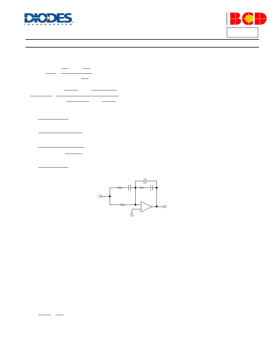
R3
V
OUT
+
-
V
REF
V
COMP
C3
C1
R2
C2
R1
FB
Figure 9.Compensation Network
The closed loop gain of the converter can be written as:
AMP
PW M
LC
Gain
Gain
Gain
Figure 10 shows the asymptotic plot of the closed loop converter gain, and the following guidelines will help to design the compensation network.
Using the below guidelines will give a compensation similar to the curve plotted. A stable closed loop has a-20dB/decade slope and a phase
margin greater than 45 degree.
1. Choose a value for R1, usually between 1k
and 5k
.
2. Select the desired zero crossover frequency.
SW
O
f
f
)
10
/
1
~
5
/
1
(
Use the following equation to calculate R2:
1
2
R
f
f
V
V
R
LC
O
IN
OSC
3. Place the first zero f
Z1
before the output LC filter double pole frequency f
LC
.
LC
Z
f
f
75
.
0
1