Ap3595, Application information, Cr f – Diodes AP3595 User Manual
Page 14: Cl f ) 2 / 1 ( 2 1, Vgain
AP3595
Document number: DS36749 Rev. 1 - 2
14 of 23
January 2014
© Diodes Incorporated
AP3595
A Product Line of
Diodes Incorporated
Application Information
(Cont.)
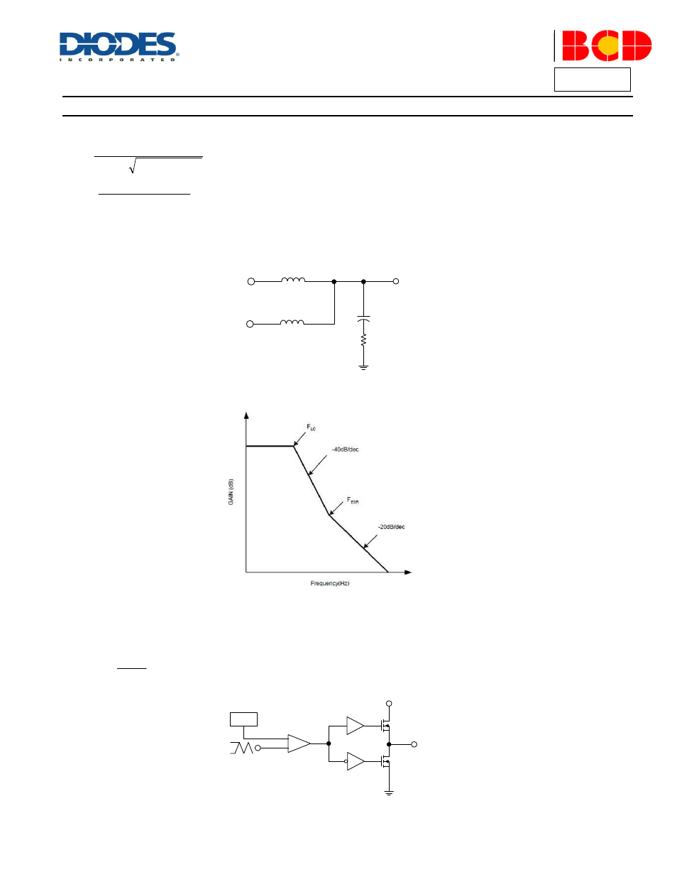
The poles and zero of the transfer functions are:
OUT
LC
C
L
f
)
2
/
1
(
2
1
OUT
ESR
ESR
C
R
f
2
1
The f
LC
is the double-pole frequency of the two-phase LC filters, and f
ESR
is the frequency of the zero introduced by the ESR of the output
capacitors.
V
PHASE1
V
PHASE2
V
OUT
C
OUT
R
ESR
L1=L
L2=L
Figure 6. The Output LC Filter
Figure 7. .Frequency Response of the LC Filters
The PWM modulator is shown in Figure 8. The input is the output of the error amplifier and the output is the PHASE node. The transfer function of
the PWM modulator is given by:
OSC
IN
PW M
V
V
Gain
+
-
PWM
Comparator
OSC
ΔV
OSC
V
IN
Driver
Driver
PHASE
Output of Error
Amplifier
Figure 8.The PWM Modulator
- PDS3200 (5 pages)
- PDS340 (5 pages)
- PDS340Q (5 pages)
- PDS360 (5 pages)
- PDS360Q (5 pages)
- PDS4150 (4 pages)
- PDS3100Q (5 pages)
- PDS3100 (5 pages)
- PDS1240CTL (5 pages)
- PDS1045 (5 pages)
- PDS1040L (5 pages)
- PDS1040CTL (5 pages)
- PDS1040 (5 pages)
- PD3S230L (5 pages)
- PD3S230H (3 pages)
- PDS5100Q (5 pages)
- PDS835L (5 pages)
- PDS760 (5 pages)
- PDS560 (5 pages)
- PDS540 (5 pages)
- PDS5100H (5 pages)
- PDS5100 (5 pages)
- PDS4200H (6 pages)
- SBL3060CTP (4 pages)
- SBL30L30CT (3 pages)
- SBL3045CTP (4 pages)
- SBL3040CTP (4 pages)
- SBL2060CTP (4 pages)
- SBL2030CT - SBL2060CT (3 pages)
- SBL2045CTP (4 pages)
- SBL1060CTP (4 pages)
- SBL1040CTP (4 pages)
- SBG3030CT - SBG3045CT (5 pages)
- SB520 - SB560 (3 pages)
- SB370 - SB3100 (3 pages)
- SB320 - SB360 (3 pages)
- SBR10U100CT (5 pages)
- SBR10U150CT (5 pages)
- SBR10A45SP5 (5 pages)
- SBR1060CT (5 pages)
- SBR1045SP5 (5 pages)
- SBR1045SD1 (4 pages)
- SBR1045D1 (5 pages)
- SBR1045CTL (4 pages)
- SBR1040CT (5 pages)