Ap3595, Functional block diagram, Absolute maximum ratings – Diodes AP3595 User Manual
Page 4
AP3595
Document number: DS36749 Rev. 1 - 2
4 of 23
January 2014
© Diodes Incorporated
AP3595
A Product Line of
Diodes Incorporated
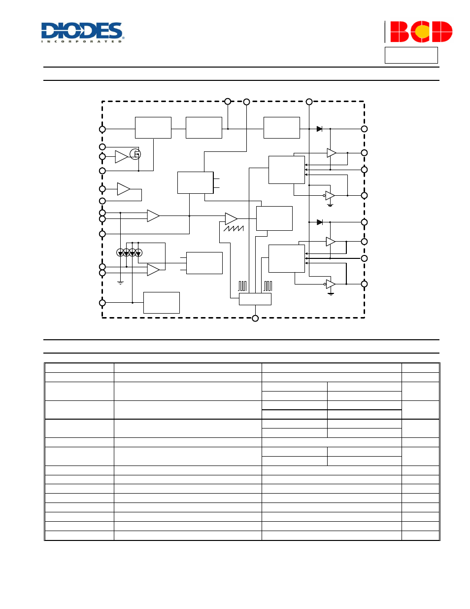
Functional Block Diagram
Reference
Voltage
POR
Internal
Regulator
Gate
Control
Logic
DUAL PHASE
Control
Gate
Control
Logic
OCP
OVP
UVP
Power Saving
Setting
Oscillator
+
-
BOOT1
HG1
PHASE1
LG1
BOOT2
HG2
LG2
PVCC
+
-
PWM
Current
Balance
RT/EN
PHASE1
PHASE2
IOFS
VREF
RSET
VID
FBRTN
REFIN
SS
EAP
FB
Error
Amplifier
COMP
+
-
CSN
CSP
PSI
FB
SS
VCC
2
24
23
1
9
8
6
5
10
11
12
3
19
20
15
21
22
16
14
13
17
4
18
PHASE2
7
Absolute Maximum Ratings
(Note 4)
Symbol
Parameter
Rating
Unit
V
CC
Supply Input Voltage
-0.3 to 15
V
V
PHASE
PHASE to GND Voltage
DC
-0.3 to 15
V
<200ns
-5 to 30
V
HG
HG to PHASE Voltage
DC
-0.3 to V
BOOT-PHASE
+0.3
V
<200ns
-5 to V
BOOT-PHASE
+5
V
LG
LG to GND Voltage
DC
-0.3 to V
CC
+0.3
V
<200ns
-5 to V
CC
+5
–
BOOT to PHASE Voltage
15
V
V
BOOT
BOOT to GND Voltage
DC
-0.3 to V
PHASE
+15
V
<200ns
-0.3 to 42
Input, Output or I/O Voltage
-0.3 to 6
V
P
D
Power Dissipation
2.5
W
JA
Thermal Resistance (Junction to Ambient)
40
°C/W
T
STG
Storage Temperature Range
-65 to +150
ºC
T
J
Junction Temperature
+150
ºC
T
LEAD
Lead Temperature (Soldering, 10sec)
+260
ºC
V
HBM
ESD (Human Body Model)
2000
V
V
MM
ESD (Machine Model)
200
V
Note 4
: Stresses greater than those listed under “Absolute Maximum Ratings” may cause permanent damage to the device. These are stress ratings only, and
functional operation of the device at these or any other conditions beyond those indicated under “Recommended Operating Conditions” is not implied.
Exposure to “Absolute Maximum Ratings” for extended periods may affect device reliability.