Ap3595, Application information, A12 10 r i i – Diodes AP3595 User Manual
Page 11
AP3595
Document number: DS36749 Rev. 1 - 2
11 of 23
January 2014
© Diodes Incorporated
AP3595
A Product Line of
Diodes Incorporated
Application Information
(Cont.)
As mentioned in the above section, the slew rate of voltage transition at SS pin and V
OUT
during soft start and V
REFIN
jumping is controlled by the
capacitor connected to the SS pin. This reduces inrush current to charge/discharge the large output capacitors during soft start and VID changing,
and prevents OCP, OVP/UVP false trigger. The SS buffer sinking/sourcing capability is limited to 22
A during soft start and 200
A after soft start
end. Therefore, the slew rate of voltage ramping up/down at SS, EAP and FB pin during soft start or VID changing is calculated as:
During Soft Start
After Soft Start
4. Pre-Bias Function
AP3595 features pre-bias start-up capability. If the output voltage is pre-biased with a voltage V
BIAS
, that accordingly makes V
FB
higher than
reference voltage ramping V
EAP
. The error amplifier keeps V
COMP
lower than the valley of the saw tooth waveform and makes PWM comparators
output low until the ramping V
EAP
catches up the feedback voltage. The IC keeps both upper and lower MOSFETs off until the first pulse takes
place.
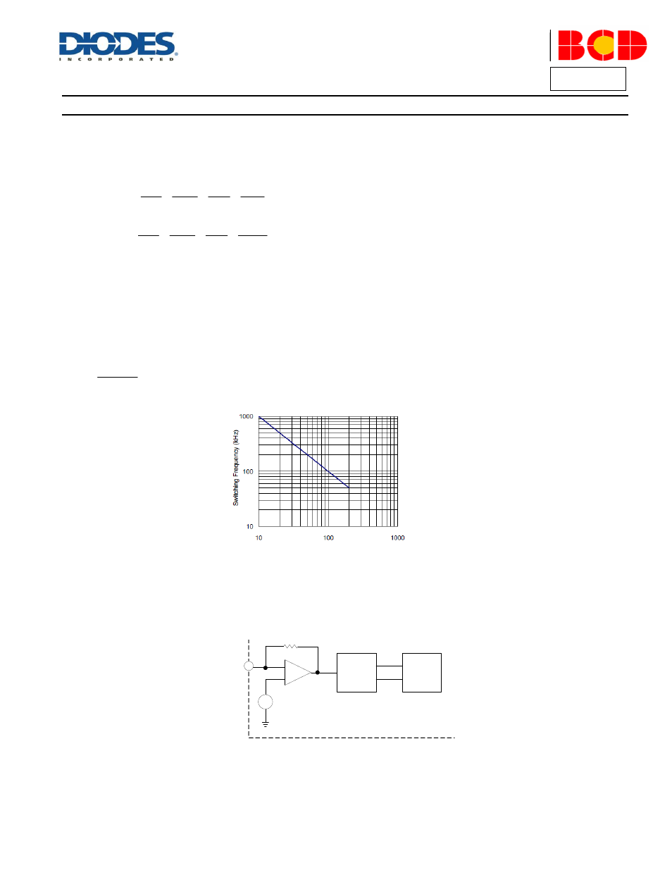
5. Chip Oscillator Frequency Programming
A resistor R
FS
connected to RT/EN pin programs the oscillator frequency as:
)
(
)
(
10000
kHz
k
R
f
FS
OSC
Figure 2 shows the relationship between oscillation frequency and R
FS
.
Figure 2. Switching Frequency vs. R
FS
When released, the RT/EN pin voltage is regulated at 1V. Pulling the RT/EN pin to ground shuts down the IC.
6. Current Balance
AP3595 extracts phase currents for current balance by parasitic on-resistance of the lower switches when turned on as shown in Figure 3.
Figure 3. R
DS(ON)
Current Sensing Scheme
The GM amplifier senses the voltage drop across the lower switch and converts it into current signal when it turns on. The sampled and held
current is expressed as:
A
12
10
R
I
I
3
)
ON
(
DS
LX
CSX
SS
FB
EAP
SS
C
A
dt
dV
dt
dV
dt
dV
22
SS
FB
EAP
SS
C
A
dt
dV
dt
dV
dt
dV
200
R
FS
(k
)
Sample
&Hold
Current
Balance
I
CS1
I
CS2
_
+
Reference
Voltage
+
_
PHASE