Ap3595, Application information – Diodes AP3595 User Manual
Page 16
AP3595
Document number: DS36749 Rev. 1 - 2
16 of 23
January 2014
© Diodes Incorporated
AP3595
A Product Line of
Diodes Incorporated
Application Information
(Cont.)
Calculate the C2 by the equation:
75
.
0
2
2
1
2
LC
f
R
C
4. Set the pole at the ESR zero frequency f
ESR
:
ESR
P
f
f
1
Calculate the C1 by the following equation:
1
2
2
2
2
1
ESR
f
C
R
C
C
5. Set the second pole f
P2
at the half of the switching frequency and also set the second zero f
Z2
at the output LC filter double pole f
LC
. The
compensation gain should not exceed the error amplifier open loop gain. Check the compensation gain at f
P2
with the capabilities of the error
amplifier.
LC
Z
SW
P
f
f
f
f
2
2
5
.
0
Combine the two equations will get the following component calculations:
1
2
1
3
LC
SW
f
f
R
R
SW
f
R
C
3
1
3
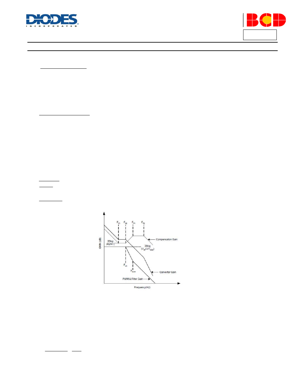
Figure 10.Converter Gain and Frequency
14. Output Inductor Selection
The duty cycle (D) of a buck converter is the function of the input voltage and output voltage. Once an output voltage is fixed, it can be written as:
IN
OUT
V
V
D
/
For two-phase converter, the inductor value (L)
determines the sum of the two inductor ripple current, ΔI
P-P
, and affects the load transient
response. Higher inductor value
reduces the output capacitors’ ripple current and induces lower output ripple voltage. The ripple current can be
approximated by:
IN
OUT
SW
OUT
IN
P
P
V
V
L
f
V
V
I
2
Where f
SW
is the switching frequency of the regulator.