Zxld1362, Electrical characteristics – Diodes ZXLD1362 User Manual
Page 4
ZXLD1362
ZXLD1362
Document number: DS33472 Rev. 5 - 2
4 of 24
May 2012
© Diodes Incorporated
A Product Line of
Diodes Incorporated
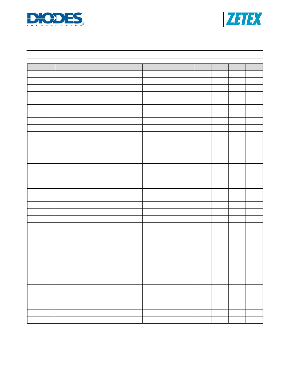
Electrical Characteristics
(Test conditions: V
IN
= 24V, T
A
= +25°C, unless otherwise specified.)
Symbol
Parameter
Condition
Min
Typ
Max
Unit
V
SU
Internal regulator start-up threshold
4.85
V
V
SD
Internal regulator shutdown threshold
4.75
V
I
INQoff
Quiescent supply current with output off
ADJ pin grounded
65
90
µA
I
INQon
Quiescent supply current with output switching
(Note 9)
ADJ pin floating, L = 68µH,
3 LEDs, f = 260kHz
1.8 mA
V
SENSE
Mean current sense threshold voltage
(Defines LED current setting accuracy)
Measured on I
SENSE
pin with
respect to V
IN
V
ADJ
= 1.25V
95 100 105 mV
V
SENSEHYS
Sense threshold hysteresis
±10
%
I
SENSE
I
SENSE
pin input current
V
SENSE
= V
IN
-0.1
4
10
µA
V
REF
Internal reference voltage
Measured on ADJ pin with
pin floating
1.25 V
ΔV
REF
/
ΔT
Temperature coefficient of V
REF
50
ppm/°C
V
ADJ
External control voltage range on ADJ pin for DC
brightness control (Note 7)
0.3
2.5
V
V
ADJoff
DC voltage on ADJ pin to switch device from active
(on) state to quiescent (off) state
V
ADJ
falling
0.15 0.2 0.27 V
V
ADJon
DC voltage on ADJ pin to switch device from
quiescent (off) state to active (on) state
V
ADJ
rising
0.2 0.25 0.3 V
R
ADJ
Resistance between ADJ pin and V
REF
0 < V
ADJ
< V
REF
V
ADJ
> V
REF
+100mV
30
10.4
50
14.2
65
18
k
Ω
I
LXmean
Continuous LX switch current
1
A
R
LX
LX switch ‘On’ resistance
@ I
LX
= 1A
0.5
1.0
Ω
I
LX(leak)
LX switch leakage current
5
µA
D
PWM(LF)
Duty cycle range of PWM signal applied to ADJ pin
during low frequency PWM dimming mode
PWM frequency <300Hz
PWM amplitude = V
REF
Measured on ADJ pin
0.001
1
Brightness control range
1000:1
DC
ADJ
DC Brightness control range
Note 10
5:1
t
SS
Soft start time
Time taken for output current
to reach 90% of final value
after voltage on ADJ pin has
risen above 0.3V. Requires
external capacitor 22nF. See
graphs for more details
2 ms
f
LX
Operating frequency
(See graphs for more details)
ADJ pin floating
L = 68µH (0.1V)
I
OUT
= 1A @ V
LED
= 3.6V
Driving 3 LEDs
300 kHz
t
ONmin
Minimum switch ‘ON’ time
LX switch ‘ON’
130
ns
t
OFFmin
Minimum switch ‘OFF’ time
LX switch ‘OFF’
70
ns
Notes:
9. Static current of device is approximately 700µA, see Graph, Page 16.
10. Ratio of maximum brightness to minimum brightness before shutdown V
REF
= 1.25/0.3. V
REF
externally driven to 2.5V, ratio 10:1.