Zxld1362, Application information (cont.) – Diodes ZXLD1362 User Manual
Page 20
ZXLD1362
ZXLD1362
Document number: DS33472 Rev. 5 - 2
20 of 24
May 2012
© Diodes Incorporated
A Product Line of
Diodes Incorporated
Application Information (cont.)
Diode Selection
For maximum efficiency and performance, the rectifier (D1)
should be a fast low capacitance Schottky diode* with low
reverse leakage at the maximum operating voltage and
temperature.
They also provide better efficiency than silicon diodes, due to a
combination of lower forward voltage and reduced recovery
time.
It is important to select parts with a peak current rating above
the peak coil current and a continuous current rating higher
than the maximum output load current. It is very important to
consider the reverse leakage of the diode when operating
above +85°C. Excess leakage will increase the power
dissipation in the device and if close to the load may create a
thermal runaway condition.
The higher forward voltage and overshoot due to reverse
recovery time in silicon diodes will increase the peak voltage
on the LX output. If a silicon diode is used, care should be
taken to ensure that the total voltage appearing on the LX pin
including supply ripple, does not exceed the specified
maximum value.
*A suitable Schottky diode would be 30BQ100PBF (IR).
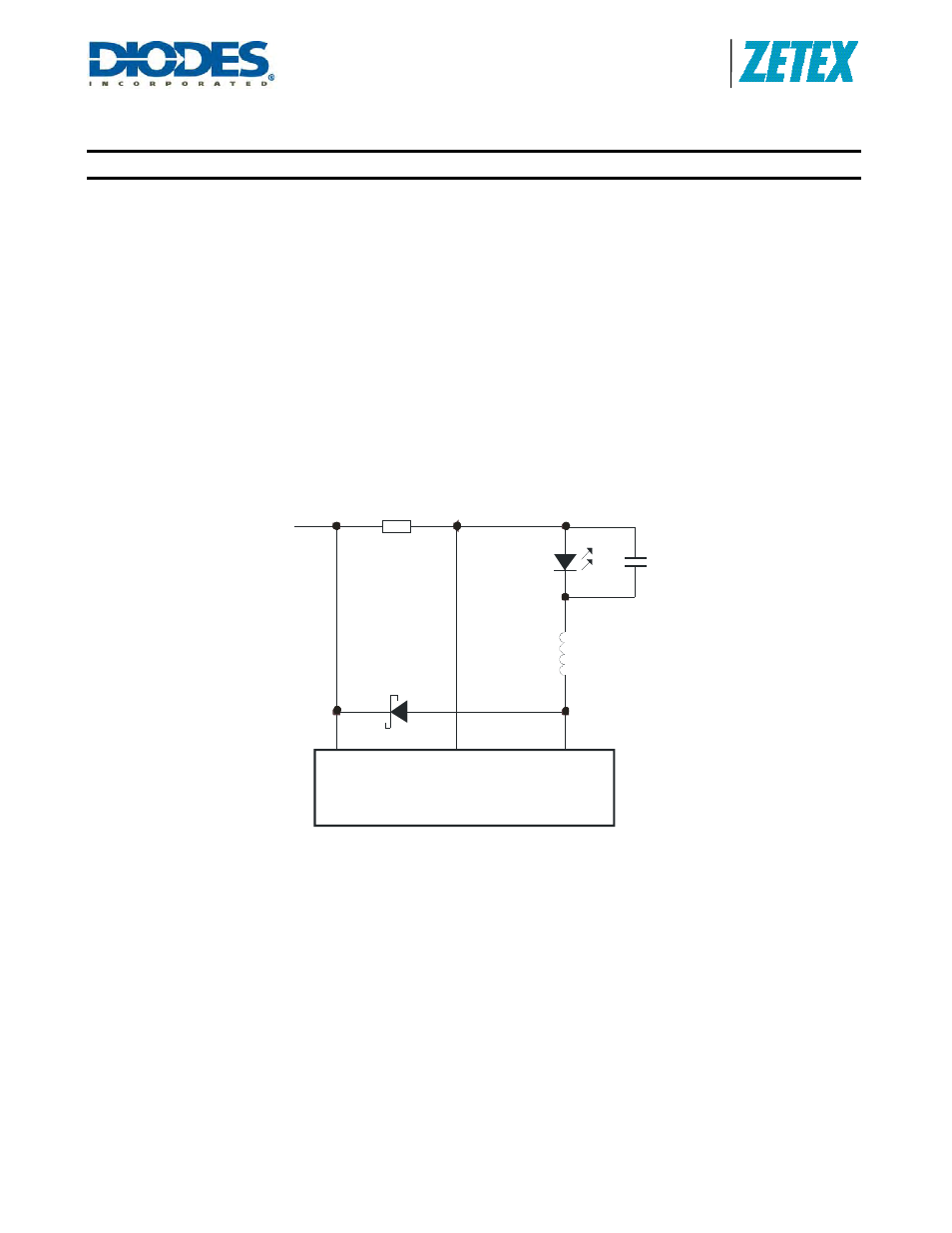
Reducing Output Ripple
Peak to peak ripple current in the LED(s) can be reduced, if
required, by shunting a capacitor Cled across the LED(s) as
shown below:
V
IN
V
IN
I
SE NSE
LX
ZXLD1362
Rs
L1
Cled
LED
D1
A value of 1
μF will reduce the supply ripple current by a factor
three (approx.). Proportionally lower ripple can be achieved
with higher capacitor values. Note that the capacitor will not
affect operating frequency or efficiency, but it will increase
start-up delay, by reducing the rate of rise of LED voltage.
By adding this capacitor the current waveform through the
LED(s) changes from a triangular ramp to a more sinusoidal
version without altering the mean current value.
Operation at Low Supply Voltage
Below the under-voltage lockout threshold (VSD) the drive to
the output transistor is turned off to prevent device operation
with excessive on-resistance of the output transistor. The
output transistor is not full enhanced until the supply voltage
exceeds approximately 17V. At supply voltages between V
SD
and 17V care must be taken to avoid excessive power
dissipation due to the on-resistance.
If the supply voltage is always less than 30V continuous an
alternative device is available, the ZXLD1360 or the AL8805.
Note that when driving loads of two or more LEDs, the forward
drop will normally be sufficient to prevent the device from
switching below approximately 6V. This will minimize the risk of
damage to the device.