Zxld1362, Pin description, Block diagram – Diodes ZXLD1362 User Manual
Page 2: A product line of diodes incorporated
ZXLD1362
ZXLD1362
Document number: DS33472 Rev. 5 - 2
2 of 24
May 2012
© Diodes Incorporated
A Product Line of
Diodes Incorporated
Pin Description
Name
Pin No.
Function
LX
1
Drain of NDMOS switch
GND 2
Ground
(0V)
ADJ 3
Multi-function On/Off and brightness control pin:
• Leave floating for normal operation.(V
ADJ
= V
REF
= 1.25V giving nominal average output current
o
I
OUTnom
= 0.1/RS)
• Drive to voltage below 0.2V to turn off output current
• Drive with DC voltage (0.3V < V
ADJ
< 2.5V) to adjust output current from 25% to 200% of I
OUTnom
• Connect a capacitor from this pin to ground to increase soft-start time.
• Soft-start time increases approximately 200µs/nF.
I
SENSE
4
Connect resistor R
S
from this pin to V
IN
to define nominal average output current I
OUTnom
= 0.1/R
S
(Note: R
SMIN
= 0.1
Ω with ADJ pin open circuit)
V
IN
5
Input voltage (6V to 60V). Decouple to ground with 4.7µF of higher X7R ceramic capacitor close to device.
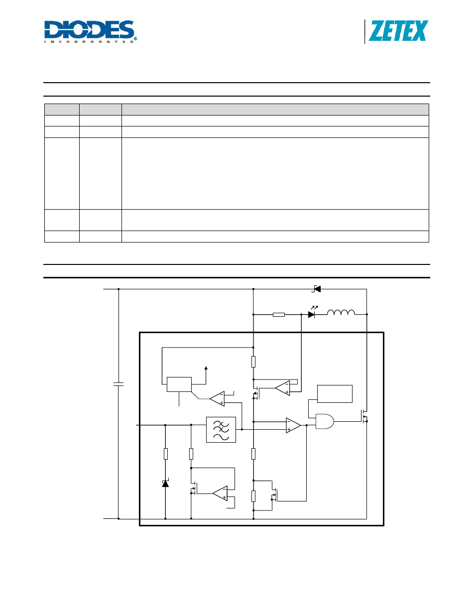
Block Diagram
Voltage
regulator
Low voltage
detector
``
L1
D1
LX
I
SENSE
V
IN
R
S
5
4
1
R1
0.2V
R2
R3
1.35V
R5
20k
R4
50k
D1
1.25V
ADJ
3
GND
2
C1
4.7µF
5V
V
IN
MN
GND
GND
Figure 1. Block Diagram