Zxld1362, Application information – Diodes ZXLD1362 User Manual
Page 17
ZXLD1362
ZXLD1362
Document number: DS33472 Rev. 5 - 2
17 of 24
May 2012
© Diodes Incorporated
A Product Line of
Diodes Incorporated
Application Information
Setting Nominal Average Output Current with External
Resistor R
S
The nominal average output current in the LED(s) is determined by
the value of the external current sense resistor (R
S
) connected
between V
IN
and I
SENSE
and is given by:
I
OUTnom
= 0.1/R
S
[for R
S
> 0.1Ω]
The table below gives values of nominal average output current for
several preferred values of current setting resistor (R
S
) in the typical
application circuit shown on page 1:
R
S
(
Ω)
Nominal average output
current (mA)
0.1 1000
0.13 760
0.15 667
The above values assume that the ADJ pin is floating and at a
nominal voltage of V
REF
(= 1.25V). Note that R
S
= 0.1
Ω is the
minimum allowed value of sense resistor under these conditions to
maintain switch current below the specified maximum value.
It is possible to use different values of R
S
if the ADJ pin is driven
from an external voltage. (See next section).
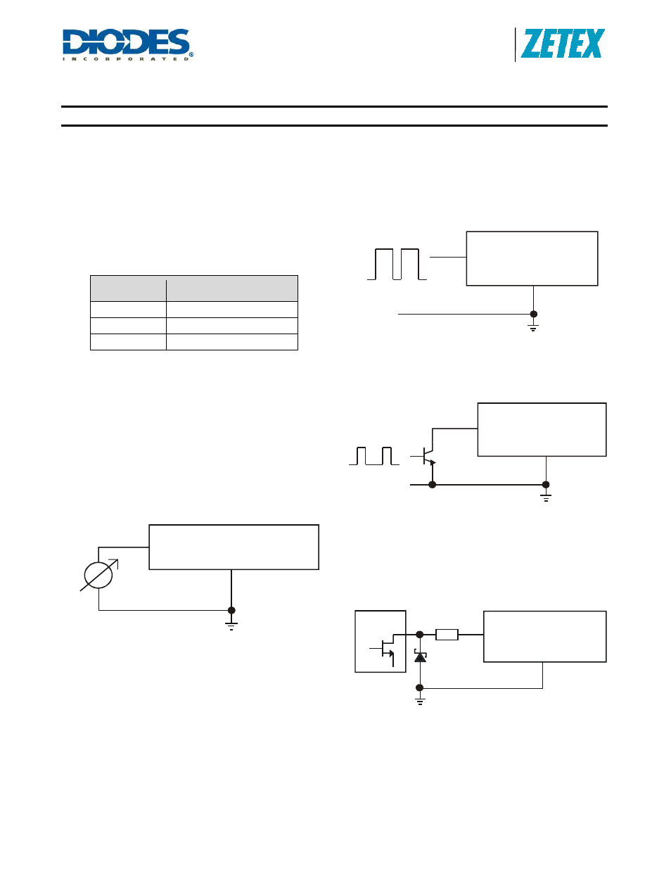
Output Current Adjustment by External DC Control
Voltage
The ADJ pin can be driven by an external dc voltage (V
ADJ
), as
shown, to adjust the output current to a value above or below the
nominal average value defined by R
S
.
The nominal average output current in this case is given by:
I
OUTdc
= (V
ADJ
/1.25) x (100mV/R
S
) [for 0.3< V
ADJ
<2.5V]
Note that 100% brightness setting corresponds to V
ADJ
= V
REF
.
When driving the ADJ pin above 1.25V, R
S
must be increased in
proportion to prevent I
OUTdc
exceeding 1A maximum.
The input impedance of the ADJ pin is 50k
Ω ±25% for voltages
below V
REF
and 14.2k
Ω ±25% for voltages above V
REF
+100mV.
Output Current Adjustment by PWM Control
Directly driving ADJ input
A Pulse Width Modulated (PWM) signal with duty cycle D
PWM
can
be applied to the ADJ pin, as shown below, to adjust the output
current to a value above or below the nominal average value set
by resistor R
S
:
Driving the ADJ Input via Open Collector Transistor
The recommended method of driving the ADJ pin and controlling
the amplitude of the PWM waveform is to use a small NPN
switching transistor as shown below:
This scheme uses the 50k resistor between the ADJ pin and the
internal voltage reference as a pull-up resistor for the external
transistor.
Driving the ADJ Input from a Microcontroller
Another possibility is to drive the device from the open drain output
of a microcontroller. The diagram below shows one method of
doing this:
If the NMOS transistor within the microcontroller has high Gate /
Drain capacitance, this arrangement can inject a negative spike
into ADJ input of the 1362 and cause erratic operation but the
addition of a Schottky clamp diode (cathode to ADJ) to ground and
inclusion of a series resistor (3.3k) will prevent this. See the
section on PWM dimming for more details of the various modes of
control using high frequency and low frequency PWM signals.
GND
ZXLD1362
ADJ
GND
+
DC
PWM
GND
0V
V
ADJ
GND
ZXLD1362
ADJ
PWM
GND
ZXLD1362
ADJ
GND
GND
Z XLD1362
ADJ
MCU
3.3k