Zxld1362, Application information (cont.) – Diodes ZXLD1362 User Manual
Page 21
ZXLD1362
ZXLD1362
Document number: DS33472 Rev. 5 - 2
21 of 24
May 2012
© Diodes Incorporated
A Product Line of
Diodes Incorporated
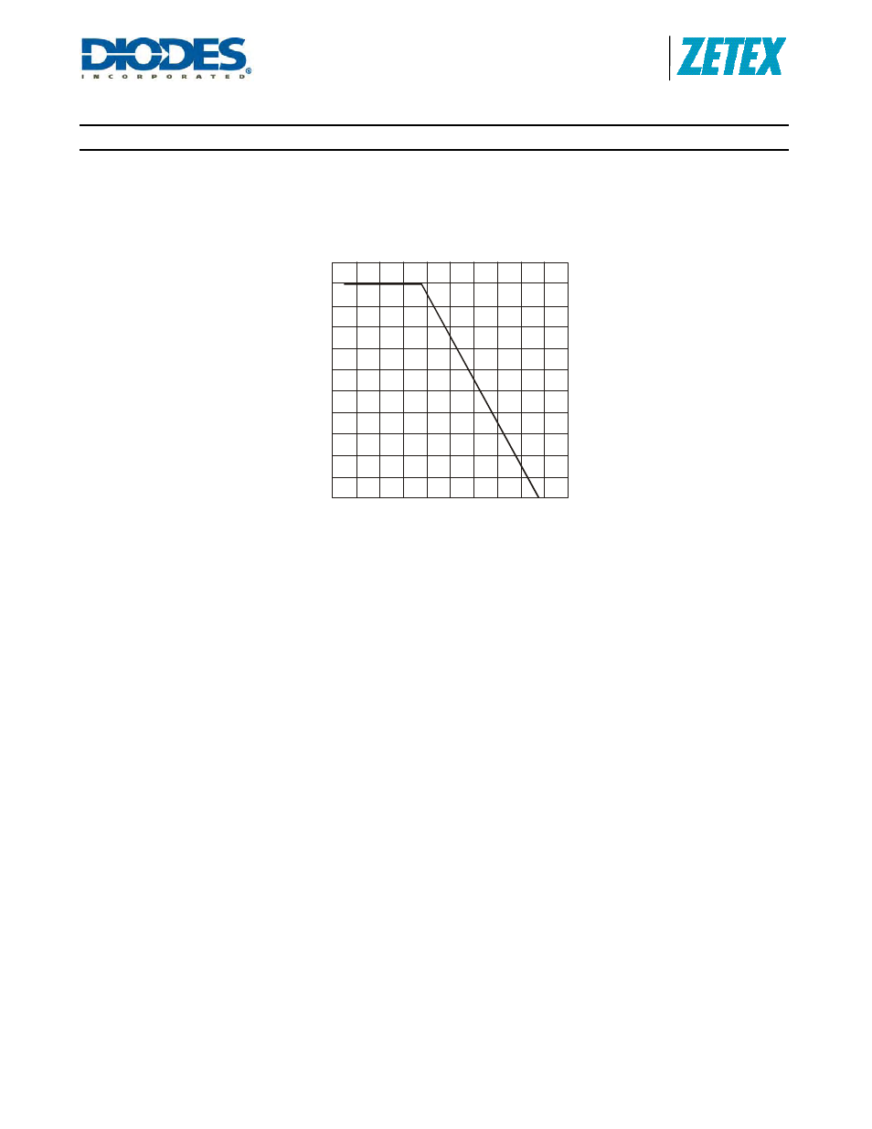
Application Information (cont.)
Thermal Considerations
When operating the device at high ambient temperatures, or
when driving maximum load current, care must be taken to
avoid exceeding the package power dissipation limits. The
graph below gives details for power derating. This assumes the
device to be mounted on a 25mm
2
PCB with 1oz copper
standing in still air.
-10 10
-50 -30
30
90 110
AMBIENT TEMPERATURE (°C)
Maximum Power Dissipation
130 150
50
70
1100
1000
900
800
500
200
100
0
700
600
P
O
WE
R
(mW
)
400
300
Note that the device power dissipation will most often be a
maximum at minimum supply voltage. It will also increase if the
efficiency of the circuit is low. This may result from the use of
unsuitable coils, or excessive parasitic output capacitance on
the switch output.
Thermal Compensation of Output Current
High luminance LEDs often need to be supplied with a
temperature compensated current in order to maintain stable
and reliable operation at all drive levels. The LEDs are usually
mounted remotely from the device so, for this reason, the
temperature coefficients of the internal circuits for the
ZXLD1362 have been optimized to minimize the change in
output current when no compensation is employed. If output
current compensation is required, it is possible to use an
external temperature sensing network - normally using
Negative Temperature Coefficient (NTC) thermistors and/or
diodes, mounted very close to the LED(s). The output of the
sensing network can be used to drive the ADJ pin in order to
reduce output current with increasing temperature.
Layout Considerations
LX Pin
The LX pin of the device is a fast switching node, so PCB
tracks should be kept as short as possible. To minimize ground
'bounce', the ground pin of the device should be soldered
directly to the ground plane.
Coil and Decoupling Capacitors and Current Sense
Resistor
It is particularly important to mount the coil and the input
decoupling capacitor as close to the device pins as possible to
minimize parasitic resistance and inductance, which will
degrade efficiency. It is also important to minimize any track
resistance in series with current sense resistor R
S
. Its best to
connect V
IN
directly to one end of R
S
and I
SENSE
directly to the
opposite end of R
S
with no other currents flowing in these
tracks. It is important that the cathode current of the Schottky
diode does not flow in a track between R
S
and V
IN
as this may
give an apparent higher measure of current than is actual
because of track resistance.