Rainbow Electronics AT24C128 User Manual
Wire serial eeproms, Features, Description
1
Features
•
Low-voltage and Standard-voltage Operation
– 2.7 (V
CC
= 2.7V to 5.5V)
– 1.8 (V
CC
= 1.8V to 3.6V)
•
Internally Organized 16,384 x 8 and 32,768 x 8
•
2-wire Serial Interface
•
Schmitt Trigger, Filtered Inputs for Noise Suppression
•
Bidirectional Data Transfer Protocol
•
1 MHz (5V), 400 kHz (2.7V, 2.5V) and 100 kHz (1.8V) Compatibility
•
Write Protect Pin for Hardware and Software Data Protection
•
64-byte Page Write Mode (Partial Page Writes Allowed)
•
Self-timed Write Cycle (5 ms Typical)
•
High Reliability
– Endurance: 100,000 Write Cycles
– Data Retention: 40 Years
•
Automotive Grade and Extended Temperature Devices Available
•
8-pin JEDEC PDIP, 8-pin JEDEC and EIAJ SOIC, 8-pin TSSOP, 14-pin TSSOP and 8-ball
dBGA
TM
Packages
Description
The AT24C128/256 provides 131,072/262,144 bits of serial electrically erasable and
programmable read only memory (EEPROM) organized as 16,384/32,768 words of 8
bits each. The device’s cascadable feature allows up to 4 devices to share a common
2-wire bus. The device is optimized for use in many industrial and commercial applica-
tions where low power and low voltage operation are essential. The devices are
available in space-saving 8-pin JEDEC PDIP, 8-pin JEDEC SOIC, 8-pin EIAJ SOIC, 8-
pin TSSOP, 14-pin TSSOP and 8-ball dBGA packages. In addition, the entire family is
available in 2.7V (2.7V to 5.5V) and 1.8V (1.8V to 3.6V) versions.
2-wire Serial
EEPROMs
128K (16,384 x 8)
256K (32,768 x 8)
AT24C128
AT24C256
Rev. 0670H–SEEPR–07/02
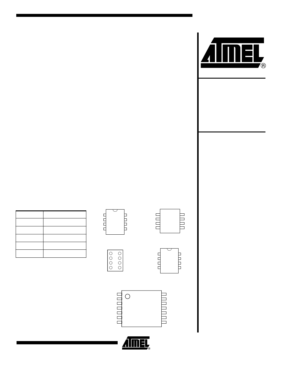
Pin Configurations
Pin Name
Function
A0 - A1
Address Inputs
SDA
Serial Data
SCL
Serial Clock Input
WP
Write Protect
NC
No Connect
8-pin PDIP
1
2
3
4
8
7
6
5
A0
A1
NC
GND
VCC
WP
SCL
SDA
8-pin SOIC
1
2
3
4
8
7
6
5
A0
A1
NC
GND
VCC
WP
SCL
SDA
14-pin TSSOP
1
2
3
4
5
6
7
14
13
12
11
10
9
8
A0
A1
NC
NC
NC
NC
GND
VCC
WP
NC
NC
NC
SCL
SDA
8-ball dBGA
Bottom View
VCC
WP
SCL
SDA
A0
A1
NC
GND
1
2
3
4
8
7
6
5
8-pin TSSOP
1
2
3
4
8
7
6
5
A0
A1
NC
GND
VCC
WP
SCL
SDA
Document Outline
- Pin Configurations
- Features
- Description
- Absolute Maximum Ratings*
- Block Diagram
- Pin Description
- Memory Organization
- Pin Capacitance(1)
- DC Characteristics(1)
- AC Characteristics
- Device Operation
- Bus Timing (SCL: Serial Clock, SDA: Serial Data I/O)
- Write Cycle Timing (SCL: Serial Clock, SDA: Serial Data I/O)
- Data Validity
- Start and Stop Definition
- Output Acknowledge
- Device Addressing
- Write Operations
- Read Operations
- AT24C128 Ordering Information
- AT24C256 Ordering Information
- Packaging Information