2 write status register – Rainbow Electronics AT26DF081A User Manual
Page 26
26
3600H–DFLASH–11/2012
AT26DF081A
10.2
Write Status Register
The Write Status Register command is used to modify the SPRL bit of the Status Register
and/or to perform a Global Protect or Global Unprotect operation. Before the Write Status Regis-
ter command can be issued, the Write Enable command must have been previously issued to
set the WEL bit in the Status Register to a logical “1”.
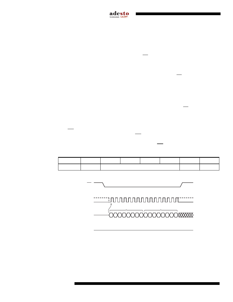
To issue the Write Status Register command, the CS pin must first be asserted and the opcode
of 01h must be clocked into the device followed by one byte of data. The one byte of data con-
sists of the SPRL bit value, a don’t care bit, four data bits to denote whether a Global Protect or
Unprotect should be performed, and two additional don’t care bits (see
). Any addi-
tional data bytes that are sent to the device will be ignored. When the CS pin is deasserted, the
SPRL bit in the Status Register will be modified, and the WEL bit in the Status Register will be
reset back to a logical “0”. The values of bits 5, 4, 3, and 2 and the state of the SPRL bit before
the Write Status Register command was executed (the prior state of the SPRL bit) will determine
whether or not a Global Protect or Global Unprotect will be performed. Please refer to the
“Global Protect/Unprotect” section on
for more details.
The complete one byte of data must be clocked into the device before the CS pin is deasserted;
otherwise, the device will abort the operation, the state of the SPRL bit will not change, no
potential Global Protect or Unprotect will be performed, and the WEL bit in the Status Register
will be reset back to the logical “0” state.
If the WP pin is asserted, then the SPRL bit can only be set to a logical “1”. If an attempt is made
to reset the SPRL bit to a logical “0” while the WP pin is asserted, then the Write Status Register
command will be ignored, and the WEL bit in the Status Register will be reset back to the logical
“0” state. In order to reset the SPRL bit to a logical “0”, the WP pin must be deasserted.
Figure 10-2. Write Status Register
Table 10-2.
Write Status Register Format
Bit 7
Bit 6
Bit 5
Bit 4
Bit 3
Bit 2
Bit 1
Bit 0
SPRL
X
Global Protect/Unprotect
X
X
SCK
CS
SI
SO
MSB
2
3
1
0
0
0
0
0
0
0
0
6
7
5
4
10 11
9
8
14 15
13
12
OPCODE
MSB
1
D
X
D
D
D
D
X
X
STATUS REGISTER IN
HIGH-IMPEDANCE