Chip erase waveforms, Page mode write waveform s – Rainbow Electronics AT28HC256 User Manual
Page 7

AT28HC256
7
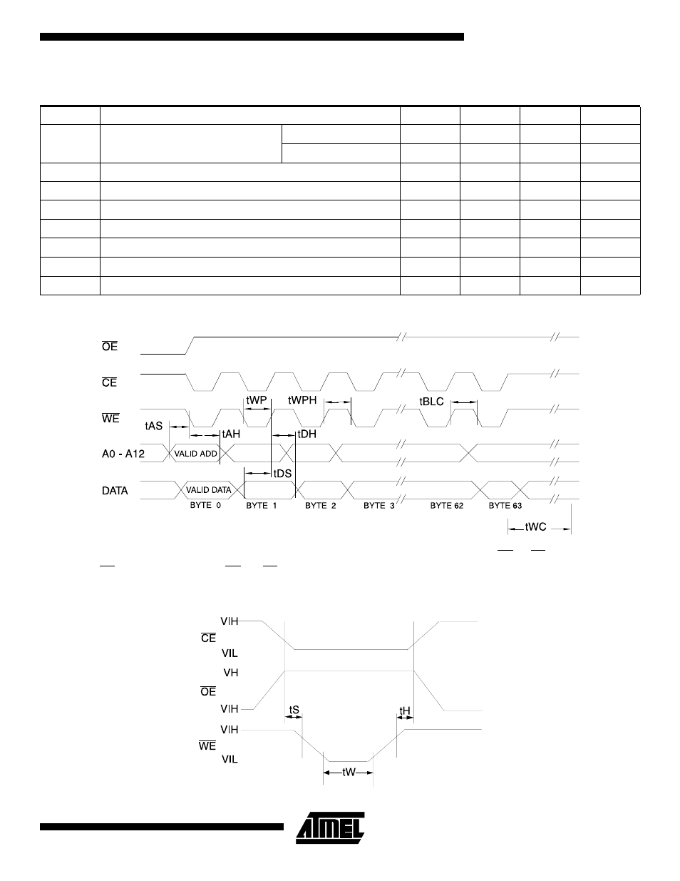
Page Mode Write Waveforms
Notes:
1.
A6 through A14 must specify the same page address during each high to low transition of WE (or CE).
2.
OE must be high only when WE and CE are both low.
Chip Erase Waveforms
Page Mode Write Characteristics
Symbol
Parameter
Min
Typ
Max
Units
t
WC
Write Cycle Time (option available)
AT28HC256
5
10
ms
AT28HC256F
2
3
ms
t
AS
Address Setup Time
0
ns
t
AH
Address Hold Time
50
ns
t
DS
Data Setup Time
50
ns
t
DH
Data Hold Time
0
ns
t
WP
Write Pulse Width
100
ns
t
BLC
Byte Load Cycle Time
150
µs
t
WPH
Write Pulse Width High
50
ns
t
S
= t
H
= 5 µsec (min.)
t
W
= 10 msec (min.)
V
H
= 12.0V
± 0.5V
See also other documents in the category Rainbow Electronics Storage:
- W27E010 (14 pages)
- W27L520 (16 pages)
- W29EE512 (21 pages)
- W27E512 (16 pages)
- W24100 (11 pages)
- W27E040 (15 pages)
- W25Q32 (60 pages)
- W49L102 (21 pages)
- W29C040 (20 pages)
- W29EE011 (20 pages)
- W49F020 (21 pages)
- W2465 (10 pages)
- W24256 (10 pages)
- W982516CH (43 pages)
- MAX16014 (12 pages)
- W24512A (10 pages)
- W27E020 (14 pages)
- W29C020C (21 pages)
- W25X64 (47 pages)
- W24257 (11 pages)
- W24L257 (10 pages)
- W9864G2GH (48 pages)
- W24L11 (11 pages)
- W27L010 (14 pages)
- W27E520 (16 pages)
- W27LE520 (16 pages)
- W9825G6CH (43 pages)
- W49F002U (23 pages)
- W9864G6GB (47 pages)
- AT45DB011B (32 pages)
- AT45DB642 (71 pages)
- AT45DB642 (37 pages)
- AT45DB161D (51 pages)
- AT27LV040A (12 pages)
- AT29LV010A (15 pages)
- HT24LC08 (11 pages)
- AT29C257 (12 pages)
- AT45DB161B (32 pages)
- AT27C1024 (12 pages)
- AT28BV256 (12 pages)
- AT28C040 (12 pages)
- DS1258Y_AB (9 pages)
- AT28BV64B (12 pages)
- AT27C512R (12 pages)
- DS1220AB_AD (9 pages)
