Rainbow Electronics AT49LV040 User Manual
Features, Description, Pin configurations
1
4-megabit
(512K x 8)
Single 2.7-volt
Battery-Voltage
™
Flash Memory
AT49BV040
AT49LV040
Features
•
Single Voltage for Read and Write: 2.7V to 3.6V (BV), 3.0V to 3.6V (LV)
•
Fast Read Access Time – 70 ns
•
Internal Program Control and Timer
•
16K Bytes Boot Block with Lockout
•
Fast Chip Erase Cycle Time – 10 seconds
•
Byte-by-byte Programming – 30 µs/Byte Typical
•
Hardware Data Protection
•
Data Polling for End of Program Detection
•
Low Power Dissipation
– 25 mA Active Current
– 50 µA CMOS Standby Current
•
Typical 10,000 Write Cycles
•
Small Packaging
– 8 x 14 mm VSOP/TSOP
Description
The AT49BV/LV040 are 3-volt only, 4-megabit Flash memories organized as 524,288
words of 8-bits each. Manufactured with Atmel’s advanced nonvolatile CMOS technol-
ogy, the devices offer access times to 70 ns with power dissipation of just 90 mW over
the commercial temperature range. When the device is deselected, the CMOS
standby current is less than 50 µA.
The device conta in s a u se r-e nab led “bo ot b lo ck” prot ectio n f eatu re . Th e
AT49BV/LV040 locates the boot block at lowest order addresses (“bottom boot”).
Rev. 0679D–03/01
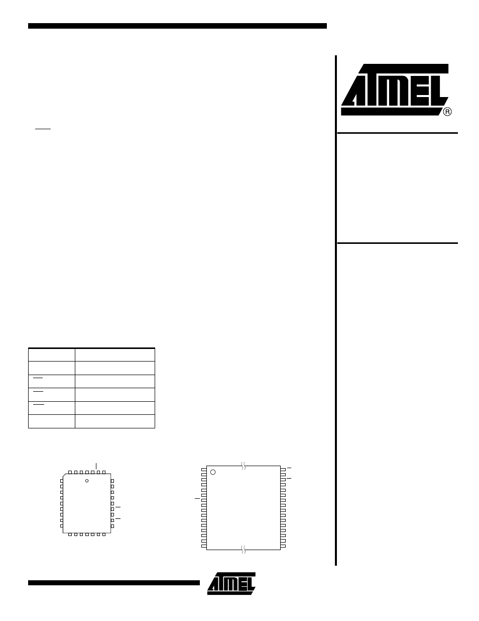
Pin Configurations
Pin Name
Function
A0 - A18
Addresses
CE
Chip Enable
OE
Output Enable
WE
Write Enable
I/O0 - I/O7
Data Inputs/Outputs
PLCC Top View
5
6
7
8
9
10
11
12
13
29
28
27
26
25
24
23
22
21
A7
A6
A5
A4
A3
A2
A1
A0
I/O0
A14
A13
A8
A9
A11
OE
A10
CE
I/O7
4
3
2
1
32
31
30
14
15
16
17
18
19
20
I/O1
I/O2
GND
I/O3
I/O4
I/O5
I/O6
A12
A15
A16
A18
VCC
WE
A17
VSOP Top View (8 x 14 mm) or
TSOP Top View (8 x 20 mm)
1
2
3
4
5
6
7
8
9
10
11
12
13
14
15
16
32
31
30
29
28
27
26
25
24
23
22
21
20
19
18
17
A11
A9
A8
A13
A14
A17
WE
VCC
A18
A16
A15
A12
A7
A6
A5
A4
OE
A10
CE
I/O7
I/O6
I/O5
I/O4
I/O3
GND
I/O2
I/O1
I/O0
A0
A1
A2
A3
(continued)
Document Outline
- Pin Configurations
- Features
- Description
- Block Diagram
- Device Operation
- Command Definition (in Hex)
- Absolute Maximum Ratings*
- DC and AC Operating Range
- Operating Modes
- DC Characteristics
- AC Read Characteristics
- AC Read Waveforms(1)(2)(3)(4)
- Input Test Waveforms and Measurement Level
- Output Test Load
- Pin Capacitance
- AC Byte Load Characteristics
- AC Byte Load Waveforms
- Program Cycle Characteristics
- Program Cycle Waveforms
- Chip Erase Cycle Waveforms
- Data Polling Characteristics(1)
- Data Polling Waveforms
- Toggle Bit Characteristics(1)
- Toggle Bit Waveforms(1)(2)(3)
- Software Product Identification Entry(1)
- Software Product Identification Exit(1)
- Boot Block Lockout Feature Enable Algorithm(1)
- AT49BV/LV040 Ordering Information