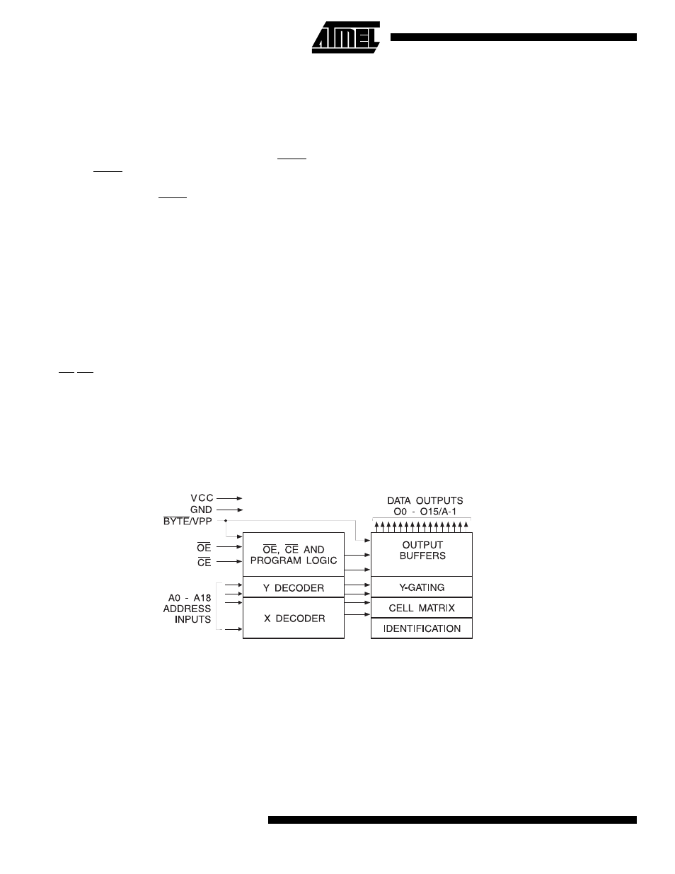
System considerations, Block diagram – Rainbow Electronics AT27C800 User Manual
Page 2
AT27C800
2
bits. It requires a single 5V power supply in normal read
mode operation. Any word can be accessed in less than 90
ns, eliminating the need for speed-reducing WAIT states.
The x16 organization makes this part ideal for high-perfor-
mance 16- and 32-bit microprocessor systems.
The AT27C800 can be organized as either word-wide or
byte-wide. The organization is selected via the BYTE/V
PP
pin. When BYTE/V
PP
is asserted high (V
IH
), the word-wide
organization is selected and the O15/A-1 pin is used for
O15 data output. When BYTE/V
PP
is asserted low (V
IL
),the
byte wide organization is selected and the O15/A-1 pin is
used for the address pin A-1. When the AT27C800 is logi-
cally regarded as x16 (word-wide), but read in the byte-
wide mode, then with A-1=V
IL
the lower eight bits of the 16
bit word are selected with A-1 =V
IH
the upper 8 bits of the
16-bit word are selected.
In read mode, the AT27C800 typically consumes 15 mA.
Standby mode supply current is typically less than 10
µ
A
.
The AT27C800 is available in industry standard JEDEC-
approved one-time programmable (OTP) PLCC, PDIP,
SOIC (SOP), and TSOP as well as UV erasable windowed
Cerdip packages. The device features two-line con-
trol(CE,OE) to eliminate bus contention in high-speed sys-
tems.
With high density 512K word or 1024K-bit storage capabil-
ity, the AT27C800 allows firmware to be to be stored reli-
ably and to be accessed by the system without the delays
of mass storage media.
Atmel’s AT27C800 has additional features that ensure high
quality and efficient production use. The Rapid
TM
Program-
ming Algorithm reduces the time required to program the
part and guarantees reliable programming. Programming
time is typically only 50
µ
s/word. The Integrated Product
Identification Code electronically identifies the device and
manufacturer. This feature is used by industry standard
programming equipment to select the proper programming
equipment and voltages.
System Considerations
Switching between active and standby conditions via the
Chip Enable pin may produce transient voltage excursions.
Unless accommodated by the system design, these tran-
sients may exceed data sheet limits, resulting in device
non-conformance. At a minimum, a 0.1
µ
F high frequency,
low inherent inductance, ceramic capacitor should be uti-
lized for each device. This capacitor should be connected
between the V
CC
and Ground terminals of the device, as
close to the device as possible. Additionally, to stabilize the
supply voltage level on printed circuit boards with large
EPROM arrays, a 4.7
µ
F bulk electrolytic capacitor should
be utilized, again connected between the V
CC
and Ground
terminals. This capacitor should be positioned as close as
possible to the point where the power supply is connected
to the array.
Block Diagram