Pin description, Data, Reset/oe – Rainbow Electronics AT17LV040 User Manual
Page 6
6
AT17LV65/128/256/512/010/002/040
2321D–CNFG–10/02
DATA
Three-state DATA output for configuration. Open-collector bi-directional pin for
programming.
CLK
Clock input. Used to increment the internal address and bit counter for reading and
programming.
WP1
WRITE PROTECT (1). Used to protect portions of memory during programming. Dis-
abled by default due to internal pull-down resistor. This input pin is not used during
FPGA loading operations. This pin is only available on AT17LV512/010/002 devices.
RESET/OE
Output Enable (active High) and RESET (active Low) when SER_EN is High. A Low
level on RESET/OE resets both the address and bit counters. A High level (with CE
Low) enables the data output driver. The logic polarity of this input is programmable as
either RESET/OE or RESET/OE. For most applications, RESET should be programmed
active Low. This document describes the pin as RESET/OE.
WP
Write protect (WP) input (when CE is Low) during programming only (SER_EN Low).
When WP is Low, the entire memory can be written. When WP is enabled (High), the
lowest block of the memory cannot be written. This pin is only available on
AT17LV65/128/256 devices.
WP2
WRITE PROTECT (2). Used to protect portions of memory during programming. Dis-
abled by default due to internal pull-down resistor. This input pin is not used during
FPGA loading operations. This pin is only available on AT17LV512/010 devices.
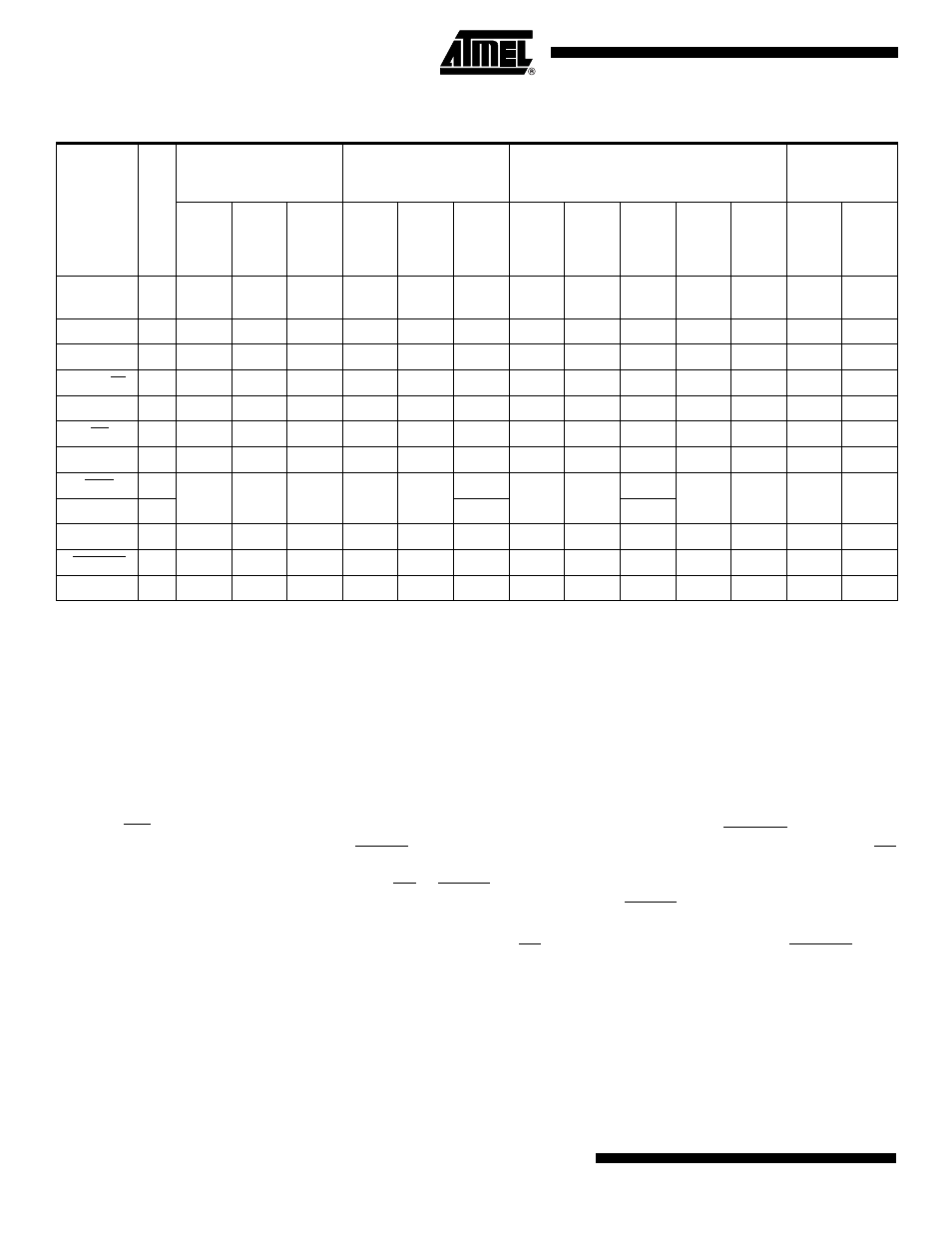
Pin Description
Name
I/O
AT17LV65/
AT17LV128/
AT17LV256
AT17LV512/
AT17LV010
AT17LV002
AT17LV040
8
DIP/
LAP/
SOIC
20
PLCC
20
SOIC
8
DIP/
LAP
20
PLCC
20
SOIC
8
DIP/
LAP/
SOIC
20
PLCC
20
SOIC
44
PLCC
44
TQFP
44
PLCC
44
TQFP
DATA
I/
O
1
2
2
1
2
1
1
2
1
2
40
2
40
CLK
I
2
4
4
2
4
3
2
4
3
5
43
5
43
WP1
I
–
–
–
–
5
–
–
5
–
–
–
–
–
RESET/OE
I
3
6
6
3
6
8
3
6
8
19
13
19
13
WP2
I
–
7
–
–
7
–
–
–
–
–
CE
I
4
8
8
4
8
10
4
8
10
21
15
21
15
GND
5
10
10
5
10
11
5
10
11
24
18
24
18
CEO
O
6
14
14
6
14
13
6
14
13
27
21
27
21
A2
I
–
–
READY
O
–
–
–
–
15
–
–
15
–
29
23
29
23
SER_EN
I
7
17
17
7
17
18
7
17
18
41
35
41
35
V
CC
8
20
20
8
20
20
8
20
20
44
38
44
38