At49f008a(t) block diagram, At49f8192a(t) block diagram, Device operation – Rainbow Electronics AT49F8192AT User Manual
Page 3
3
AT49F008A(T)/8192A(T)
1199F–04/01
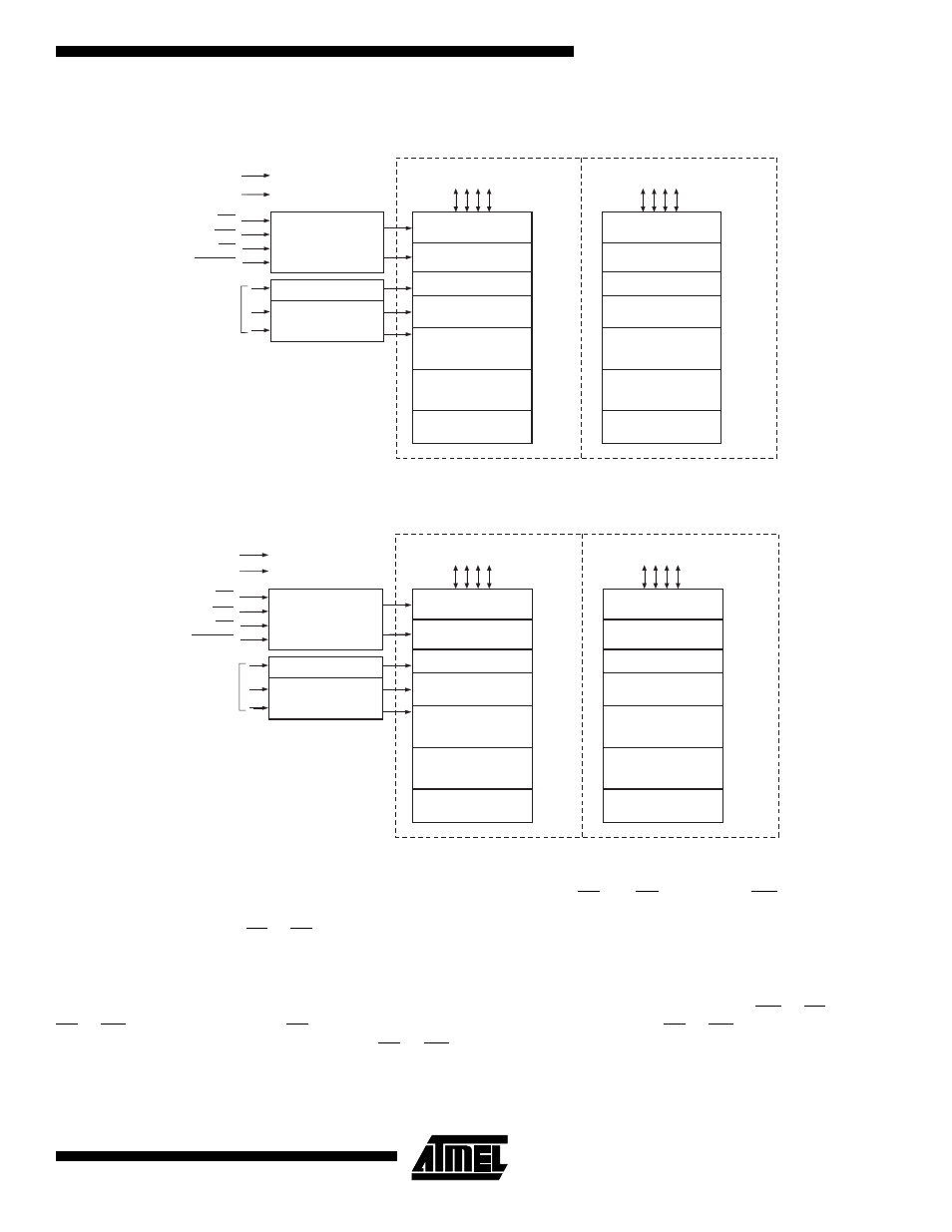
AT49F008A(T) Block Diagram
AT49F8192A(T) Block Diagram
Device Operation
READ: The AT49F008A(T)/8192A(T) is accessed like an EPROM. When CE and OE are low and WE is high, the data
stored at the memory location determined by the address pins is asserted on the outputs. The outputs are put in the high-
impedance state whenever CE or OE is high. This dual line control gives designers flexibility in preventing bus contention.
COMMAND SEQUENCES: When the device is first powered on, it will be reset to the read or standby mode, depending
upon the state of the control line inputs. In order to perform other device functions, a series of command sequences are
entered into the device. The command sequences are shown in the Command Definitions table (I/O8 - I/O15 are don’t care
inputs for the command codes). The command sequences are written by applying a low pulse on the WE or CE input with
CE or WE low (respectively) and OE high. The address is latched on the falling edge of CE or WE, whichever occurs last.
The data is latched by the first rising edge of CE or WE. Standard microprocessor write timings are used. The address
locations used in the command sequences are not affected by entering the command sequences.
VCC
GND
OE
CONTROL
LOGIC
DATA INPUTS/OUTPUTS
I/O0 - I/O7
DATA INPUTS/OUTPUTS
I/O0 - I/O7
WE
CE
RESET
ADDRESS
INPUTS
Y DECODER
INPUT/OUTPUT
BUFFERS
INPUT/OUTPUT
BUFFERS
PROGRAM DATA
LATCHES
PROGRAM DATA
LATCHES
Y-GATING
AT49F008A
AT49F008AT
Y-GATING
FFFFF
FFFFF
MAIN MEMORY
(992K BYTES)
BOOT BLOCK
16K BYTES
PARAMETER
BLOCK 2
8K BYTES
PARAMETER
BLOCK 1
8K BYTES
PARAMETER
BLOCK 1
8K BYTES
PARAMETER
BLOCK 2
8K BYTES
BOOT BLOCK
16K BYTES
MAIN MEMORY
(992K BYTES)
08000
07FFF
FC000
FBFFF
06000
05FFF
FA000
F9FFF
X DECODER
04000
03FFF
F8000
F7FFF
00000
00000
VCC
GND
OE
CONTROL
LOGIC
DATA INPUTS/OUTPUTS
I/O0 - I/O15
DATA INPUTS/OUTPUTS
I/O0 - I/O15
WE
CE
RESET
ADDRESS
INPUTS
Y DECODER
INPUT/OUTPUT
BUFFERS
INPUT/OUTPUT
BUFFERS
PROGRAM DATA
LATCHES
PROGRAM DATA
LATCHES
Y-GATING
AT49F8192A
AT49F8192AT
Y-GATING
7FFFF
7FFFF
MAIN MEMORY
(496K WORDS)
BOOT BLOCK
8K WORDS
PARAMETER
BLOCK 2
4K WORDS
PARAMETER
BLOCK 1
4K WORDS
PARAMETER
BLOCK 1
4K WORDS
PARAMETER
BLOCK 2
4K WORDS
BOOT BLOCK
8K WORDS
MAIN MEMORY
(496K WORDS)
04000
03FFF
7E000
7DFFF
03000
02FFF
7D000
7CFFF
X DECODER
02000
01FFF
7C000
7BFFF
00000
00000