Program cycle characteristics, Program cycle waveforms, Sector or chip erase cycle waveforms – Rainbow Electronics AT49F8192AT User Manual
Page 10
10
AT49F008A(T)/8192A(T)
1199F–04/01
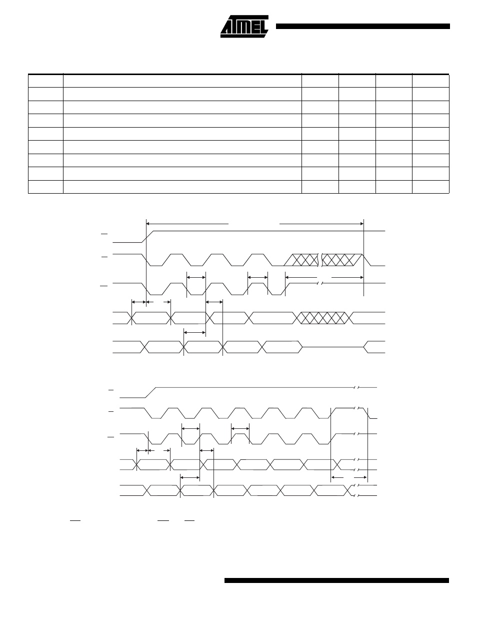
Program Cycle Waveforms
Sector or Chip Erase Cycle Waveforms
Notes:
1.
OE must be high only when WE and CE are both low.
2.
For chip erase, the address should be 5555. For sector erase, the address depends on what sector is to be erased.
(See note 4 under Command Definitions.)
3.
For chip erase, the data should be 10H, and for sector erase, the data should be 30H.
Program Cycle Characteristics
Symbol
Parameter
Min
Typ
Max
Units
t
BP
Byte/Word Programming Time
10
50
µs
t
AS
Address Setup Time
0
ns
t
AH
Address Hold Time
50
ns
t
DS
Data Setup Time
50
ns
t
DH
Data Hold Time
0
ns
t
WP
Write Pulse Width
50
ns
t
WPH
Write Pulse Width High
40
ns
t
EC
Erase Cycle Time
5
seconds
OE
INPUT DATA
ADDRESS
A0
55
5555
5555
AA
2AAA
t BP
t WPH
t WP
CE
WE
t
AS
tAH
t DH
t DS
5555
AA
PROGRAM CYCLE
A0-A18
DATA
OE
(1)
AA
80
55
55
5555
5555
AA
2AAA
2AAA
t
WPH
t
WP
CE
WE
t AS
tAH
t EC
t DH
t DS
5555
A0-A18
DATA
Note 2
Note 3
BYTE/
WORD 0
BYTE/
WORD 1
BYTE/
WORD 2
BYTE/
WORD 3
BYTE/
WORD 4
BYTE/
WORD 5