Reading the signature bytes, Parallel programming characteristics – Rainbow Electronics AT90LS4433 User Manual
Page 92

92
AT90S/LS4433
1042G–AVR–09/02
Reading the Signature Bytes
The algorithm for reading the signature bytes is as follows (refer to “Programming the
Flash” for details on command and address loading):
A: Load Command “0000 1000”.
B: Load Address Low Byte ($00 - $02).
1.
Set OE to “0”, and BS to “0”. The selected signature byte can now be read at
DATA.
2.
Set OE to “1”.
Parallel Programming
Characteristics
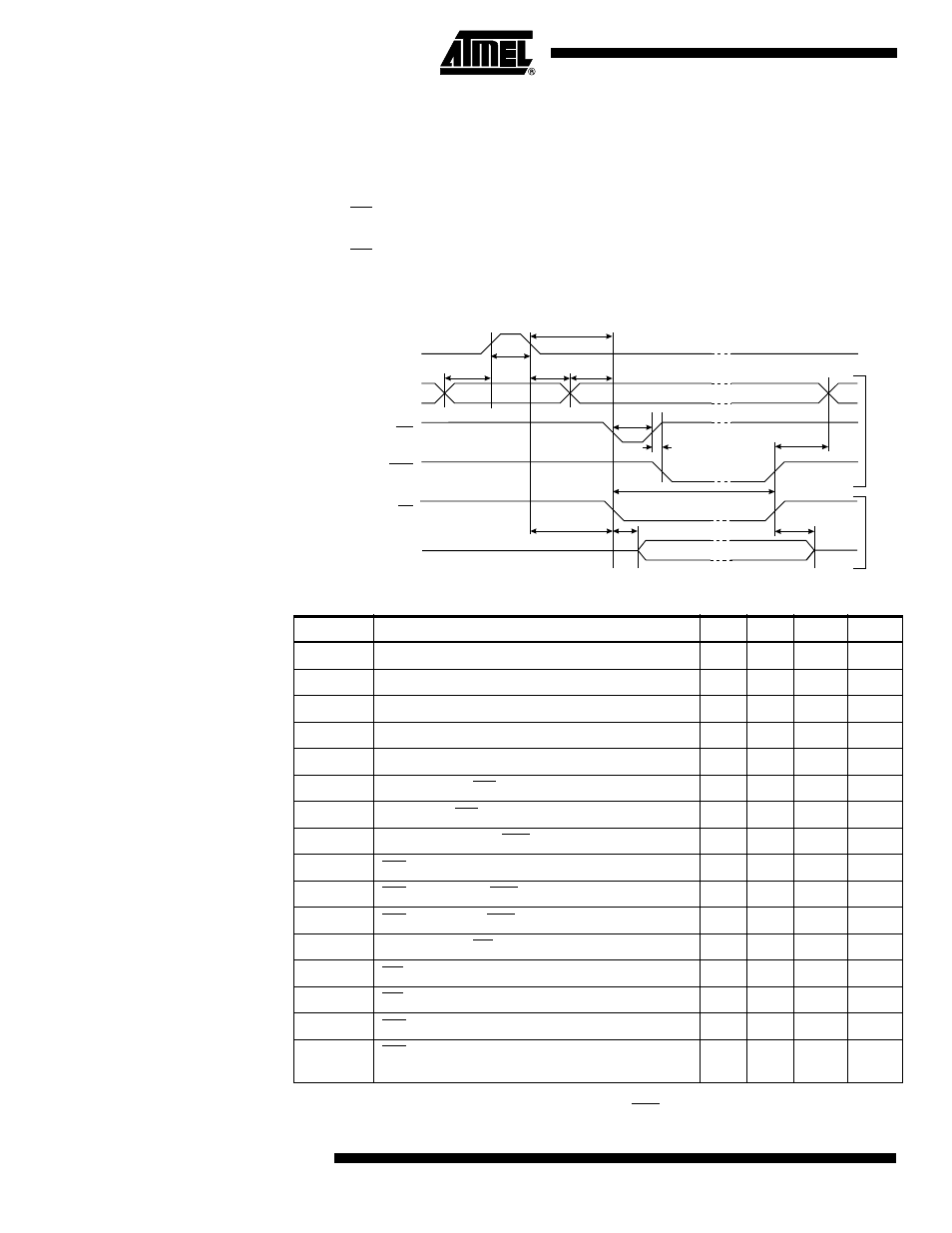
Figure 65. Parallel Programming Timing
Notes:
1. Use t
WLWH_CE
for Chip Erase and t
WLWH_PFB
for programming the Fuse bits.
2. If t
WLWH
is held longer than t
WLRH
, no RDY/BSY pulse will be seen.
Table 33. Parallel Programming Characteristics T
A
= 25
°C ± 10%, V
CC
= 5V ± 10%
Symbol
Parameter
Min
Typ
Max
Units
V
PP
Programming Enable Voltage
11.5
12.5
V
I
PP
Programming Enable Current
250.0
µA
t
DVXH
Data and Control Setup before XTAL1 High
67.0
ns
t
XHXL
XTAL1 Pulse Width High
67.0
ns
t
XLDX
Data and Control Hold after XTAL1 Low
67.0
ns
t
XLWL
XTAL1 Low to WR Low
67.0
ns
t
BVWL
BS Valid to WR Low
67.0
ns
t
RHBX
BS Hold after RDY/BSY High
67.0
ns
t
WLWH
WR Pulse Width Low
(1)
67.0
ns
t
WHRL
WR High to RDY/BSY Low
(2)
20.0
ns
t
WLRH
WR Low to RDY/BSY High
(2)
0.5
0.7
0.9
ms
t
XLOL
XTAL1 Low to OE Low
67.0
ns
t
OLDV
OE Low to DATA Valid
20.0
ns
t
OHDZ
OE High to DATA Tri-stated
20.0
ns
t
WLWH_CE
WR Pulse Width Low for Chip Erase
5.0
10.0
15.0
ms
t
WLWH_PFB
WR Pulse Width Low for Programming the Fuse
Bits
1.0
1.5
1.8
ms
Data & Contol
(DATA, XA0/1, BS)
DATA
W
rite
Read
XTAL1
t
XHXL
t
WLWH
t
DVXH
t
XLOL
t
OLDV
t
WHRL
t
WLRH
WR
RDY/BSY
OE
t
XLDX
t
XLWL
t
RHBX
t
OHDZ
t
BVWL
