Serial peripheral interface – spi – Rainbow Electronics AT90LS4433 User Manual
Page 48
48
AT90S/LS4433
1042G–AVR–09/02
Serial Peripheral
Interface – SPI
The Serial Peripheral Interface (SPI) allows high-speed synchronous data transfer
between the AT90S4433 and peripheral devices or between several AVR devices. The
AT90S4433 SPI features include the following:
•
Full Duplex, Three-wire Synchronous Data Transfer
•
Master or Slave Operation
•
LSB First or MSB First Data Transfer
•
Four Programmable Bit Rates
•
End of Transmission Interrupt Flag
•
Write Collision Flag Protection
•
Wake-up from Idle Mode
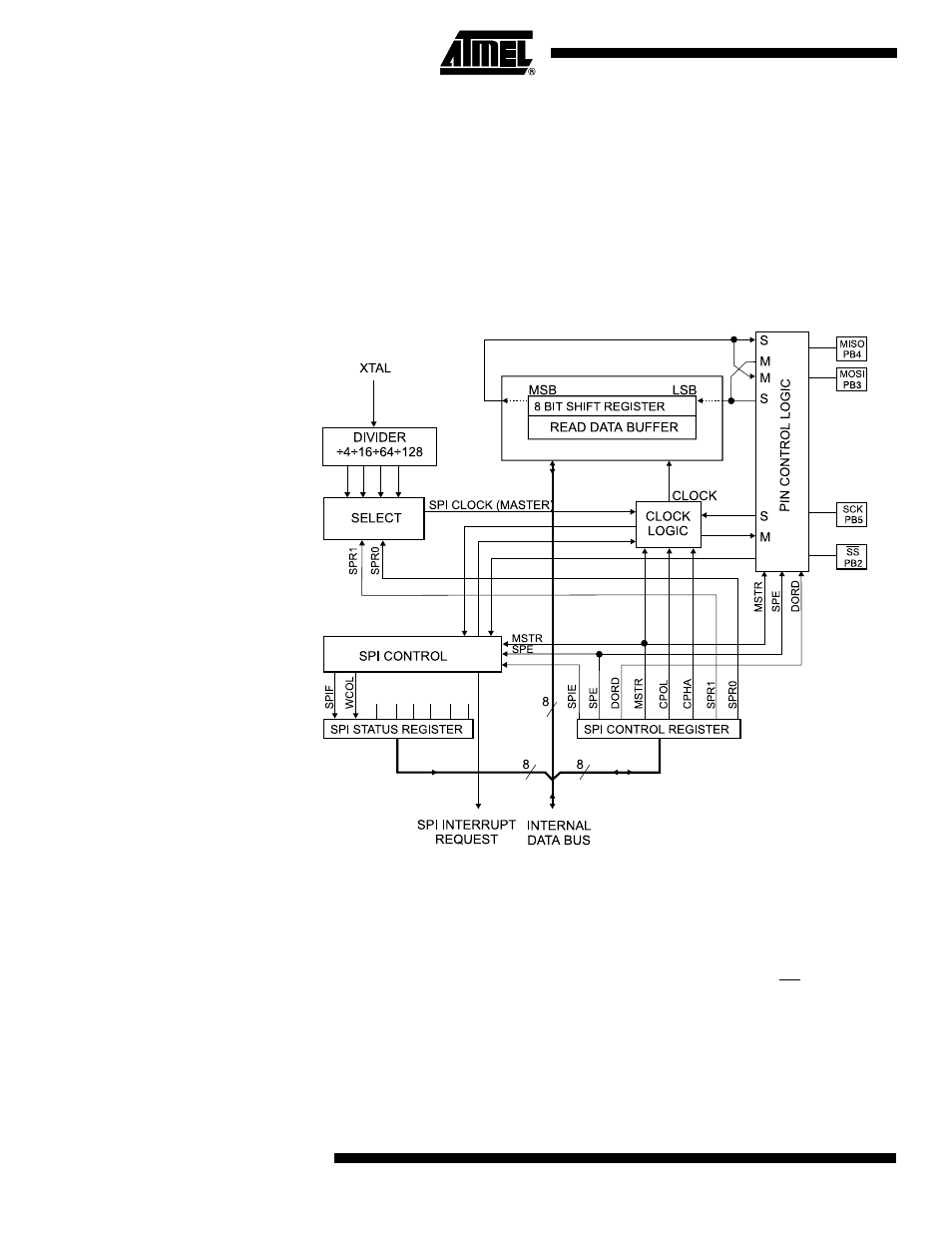
Figure 36. SPI Block Diagram
The interconnection between Master and Slave CPUs with SPI is shown in Figure 37.
The PB5(SCK) pin is the clock output in the Master mode and is the clock input in the
Slave mode. Writing to the SPI Data Register of the Master CPU starts the SPI clock
generator, and the data written shifts out of the PB3(MOSI) pin and into the PB3(MOSI)
pin of the Slave CPU. After shifting one byte, the SPI clock generator stops, setting the
end of Transmission Flag (SPIF). If the SPI Interrupt Enable bit (SPIE) in the SPCR
Register is set, an interrupt is requested. The Slave Select input, PB2(SS), is set low to
select an individual Slave SPI device. The two Shift Registers in the Master and the
Slave can be considered as one distributed 16-bit circular Shift Register. This is shown
in Figure 37. When data is shifted from the Master to the Slave, data is also shifted in
the opposite direction, simultaneously. This means that during one shift cycle, data in
the master and the slave are interchanged.