Port c, Figure 55. port b schematic diagram (pin pb5) – Rainbow Electronics AT90LS4433 User Manual
Page 77
77
AT90S/LS4433
1042G–AVR–09/02
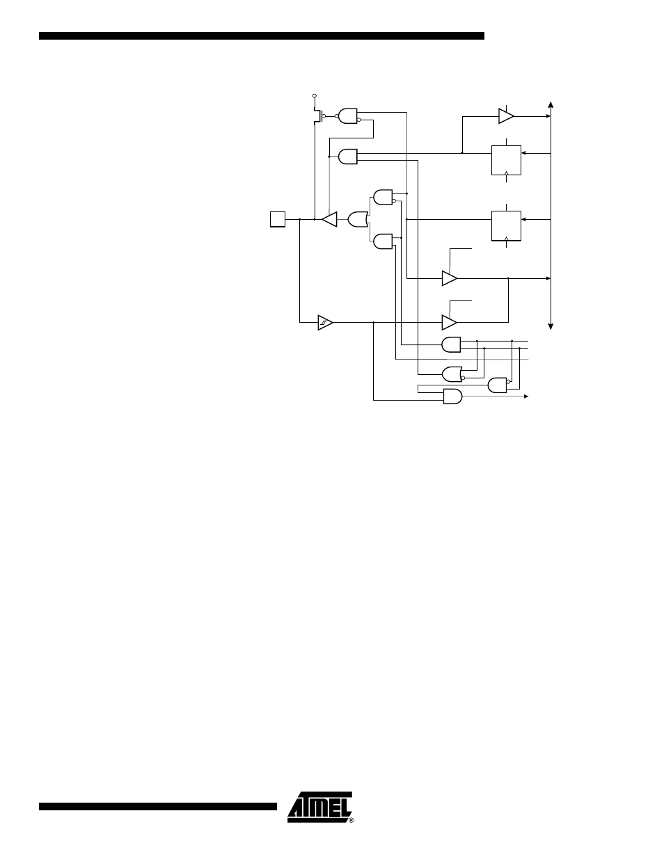
Figure 55. Port B Schematic Diagram (Pin PB5)
Port C
Port C is a 6-bit bi-directional I/O port.
Three I/O memory address locations are allocated for the Port C, one each for the Data
Register – PORTC, $15($35), Data Direction Register – DDRC, $14($34), and the Port
C Input Pins – PINC, $13($33). The Port C Input Pins address is read only, while the
Data Register and the Data Direction Register are read/write.
All port pins have individually selectable pull-up resistors. The Port C output buffers can
sink 20 mA and thus drive LED displays directly. When pins PC0 to PC5 are used as
inputs and are externally pulled low, they will source current if the internal pull-up resis-
tors are activated.
Port C has an alternate function as analog inputs for the ADC. If some Port C pins are
configured as outputs, it is essential that these do not switch when a conversion is in
progress. This might corrupt the result of the conversion.
During Power-down mode, the Schmitt triggers of the digital inputs are disconnected.
This allows an analog voltage close to V
CC
/2 to be present during Power-down without
causing excessive power consumption.
DA
T
A
BUS
D
D
Q
Q
RESET
RESET
C
C
WD
WP
RD
MOS
PULL-
UP
PB5
R
R
WP:
WD:
RL:
RP:
RD:
SPE:
MSTR
WRITE PORTB
WRITE DDRB
READ PORTB LATCH
READ PORTB PIN
READ DDRB
SPI ENABLE
MASTER SELECT
DDB5
PORTB5
SPE
MSTR
SPI CLOCK
OUT
SPI CLOCK
IN
RL
RP