Rainbow Electronics AT90LS4433 User Manual
Page 74
74
AT90S/LS4433
1042G–AVR–09/02
controlled by DDB2. When the pin is forced to be an input, the pull-up can still be con-
trolled by the PORTB2 bit. See the description of the SPI port for further details.
• OC1 – Port B, Bit 1
OC1, Output Compare Match output: PB1 pin can serve as an external output for the
Timer/Counter1 Output Compare. The pin has to be configured as an output (DDB1 set
[one]) to serve this function. See the timer description on how to enable this function.
The OC1 pin is also the output pin for the PWM mode timer function.
• ICP – Port B, Bit 0
ICP, Input Capture Pin: PB0 pin can serve as an external input for the Timer/Counter1
input capture. The pin has to be configured as an input (DDB0 cleared [zero]) to serve
this function. See the timer description on how to enable this function.
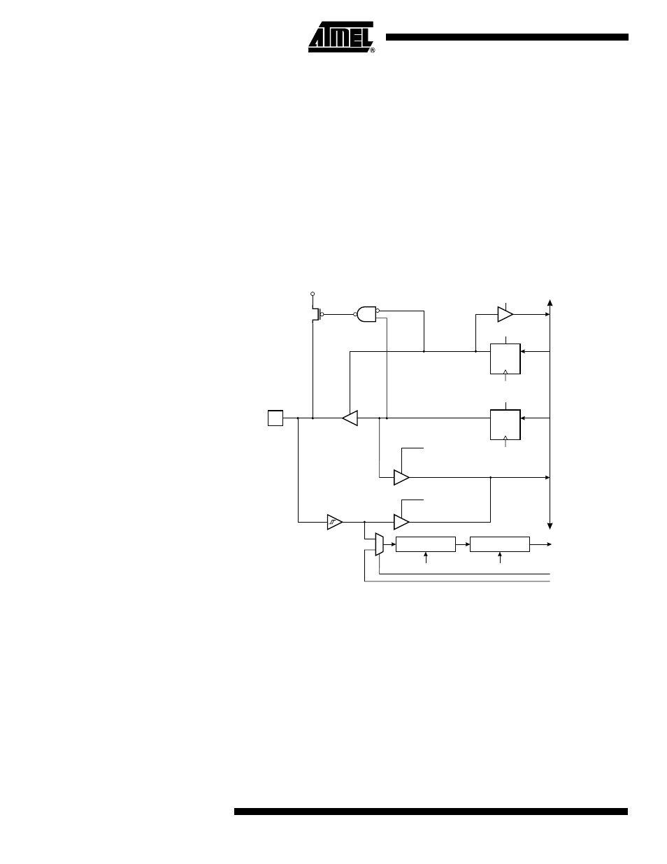
Figure 50. Port B Schematic Diagram (Pin PB0)
DA
T
A
BUS
D
D
Q
Q
RESET
RESET
C
C
WD
WP
RD
MOS
PULL-
UP
PB0
R
R
WP:
WD:
RL:
RP:
RD:
ACIC:
ACO:
WRITE PORTB
WRITE DDRB
READ PORTB LATCH
READ PORTB PIN
READ DDRB
COMPARATOR IC ENABLE
COMPARATOR OUTPUT
DDB6
PORTB0
NOISE CANCELER
EDGE SELECT
ICF1
ICNC1
ICES1
0
1
ACIC
ACO
RL
RP