Adc multiplexer select register – admux, Adc control and status register – adcsr – Rainbow Electronics AT90LS4433 User Manual
Page 68

68
AT90S/LS4433
1042G–AVR–09/02
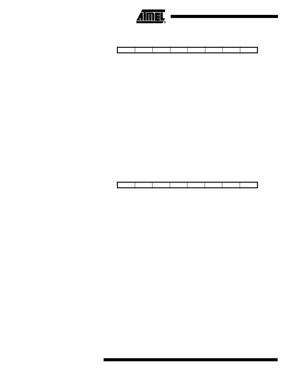
ADC Multiplexer Select
Register – ADMUX
• Bit 7 – Res: Reserved Bit
This bit is a reserved bit in the AT90S4433, and should be written to zero if accessed.
• Bit 6 – ADCBG: ADC Bandgap Select
When this bit is set and the BOD is enabled (BODEN Fuse is programmed), a fixed
bandgap voltage of 1.22V ± 0.1V replaces the normal input to the ADC. When this bit is
cleared, the normal input pin (as selected by MUX2..MUX0) is applied to the ADC.
• Bits 5..3 – Res: Reserved Bits
These bits are reserved bits in the AT90S4433, and should be written to zero if
accessed.
• Bits 2..0 – MUX2..MUX0: Analog Channel Select Bits 2 - 0
The value of these three bits selects which analog input 5 - 0 is connected to the ADC.
ADC Control and Status
Register – ADCSR
‘
• Bit 7 – ADEN: ADC Enable
Writing a logical “1” to this bit enables the ADC. By clearing this bit to zero, the ADC is
turned off. Turning the ADC off while a conversion is in progress will terminate this
conversion.
• Bit 6 – ADSC: ADC Start Conversion
In Single Conversion mode, a logical “1” must be written to this bit to start each conver-
sion. In Free Run mode, a logical “1” must be written to this bit to start the first
conversion. The first time ADSC has been written after the ADC has been enabled, or if
ADSC is written at the same time as the ADC is enabled, a dummy conversion will pre-
cede the initiated conversion. This dummy conversion performs initialization of the ADC.
ADSC remains high during the conversion. ADSC goes low after the conversion is com-
plete, but before the result is written to the ADC Data Registers. This allows a new
conversion to be initiated before the current conversion is complete. The new conver-
sion will then start immediately after the current conversion completes. When a dummy
conversion precedes a real conversion, ADSC will stay high until the real conversion
completes.
Writing a “0” to this bit has no effect.
Bit
7
6
5
4
3
2
1
0
$07 ($27)
–
ADCBG
–
–
–
MUX2
MUX1
MUX0
ADMUX
Read/Write
R
R/W
R
R
R
R/W
R/W
R/W
Initial Value
0
0
0
0
0
0
0
0
Bit
7
6
5
4
3
2
1
0
$06 ($26)
ADEN
ADSC
ADFR
ADIF
ADIE
ADPS2
ADPS1
ADPS0
ADCSR
Read/Write
R/W
R/W
R/W
R/W
R/W
R/W
R/W
R/W
Initial Value
0
0
0
0
0
0
0
0
