Eeprom read/write access, Eeprom address register – eear, Eeprom data register – eedr – Rainbow Electronics AT90LS4433 User Manual
Page 45: Eeprom control register – eecr
45
AT90S/LS4433
1042G–AVR–09/02
EEPROM Read/Write
Access
The EEPROM Access Registers are accessible in the I/O space.
The write access time is in the range of 2.5 - 4 ms, depending on the V
CC
voltages. A
self-timing function lets the user software detect when the next byte can be written. A
special EEPROM Ready interrupt can be set to trigger when the EEPROM is ready to
accept new data.
An ongoing EEPROM write operation will complete even if a reset condition occurs.
In order to prevent unintentional EEPROM writes, a two-state write procedure must be
followed. Refer to the description of the EEPROM Control Register for details on this.
When the EEPROM is written, the CPU is halted for two clock cycles before the next
instruction is executed.
When the EEPROM is read, the CPU is halted for four clock cycles before the next
instruction is executed.
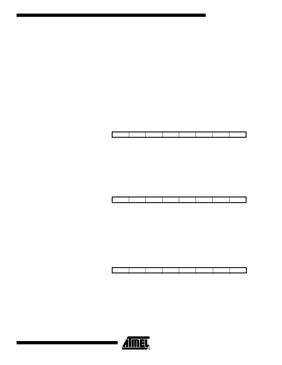
EEPROM Address Register –
EEAR
The EEPROM Address Register (EEAR) specifies the EEPROM address in the 256
bytes of EEPROM space. The EEPROM data bytes are addressed linearly between 0
and 255. The Initial Value of EEAR is undefined. A proper value must be written before
the EEPROM may be accessed.
EEPROM Data Register –
EEDR
• Bits 7..0 – EEDR7.0: EEPROM Data
For the EEPROM write operation, the EEDR Register contains the data to be written to
the EEPROM in the address given by the EEAR Register. For the EEPROM read oper-
ation, the EEDR contains the data read out from the EEPROM at the address given by
EEAR.
EEPROM Control Register –
EECR
• Bits 7..4 – Res: Reserved Bits
These bits are reserved bits in the AT90S4433 and will always read as zero.
Bit
7
6
5
4
3
2
1
0
$1E ($3E)
EEAR7
EEAR6
EEAR5
EEAR4
EEAR3
EEAR2
EEAR1
EEAR0
EEAR
Read/Write
R/W
R/W
R/W
R/W
R/W
R/W
R/W
R/W
Initial Value
X
X
X
X
X
X
X
X
Bit
7
6
5
4
3
2
1
0
$1D ($3D)
MSB
LSB
EEDR
Read/Write
R/W
R/W
R/W
R/W
R/W
R/W
R/W
R/W
Initial Value
0
0
0
0
0
0
0
0
Bit
7
6
5
4
3
2
1
0
$1C ($3C)
–
–
–
–
EERIE
EEMWE
EEWE
EERE
EECR
Read/Write
R
R
R
R
R/W
R/W
R/W
R/W
Initial Value
0
0
0
0
0
0
0
0