2 program sector protection register command – Rainbow Electronics AT45DB011D User Manual
Page 15

15
3639J–DFLASH–11/2012
AT45DB011D
9.1.2
Program Sector Protection Register Command
Once the Sector Protection Register has been erased, it can be reprogrammed using the
Program Sector Protection Register command.
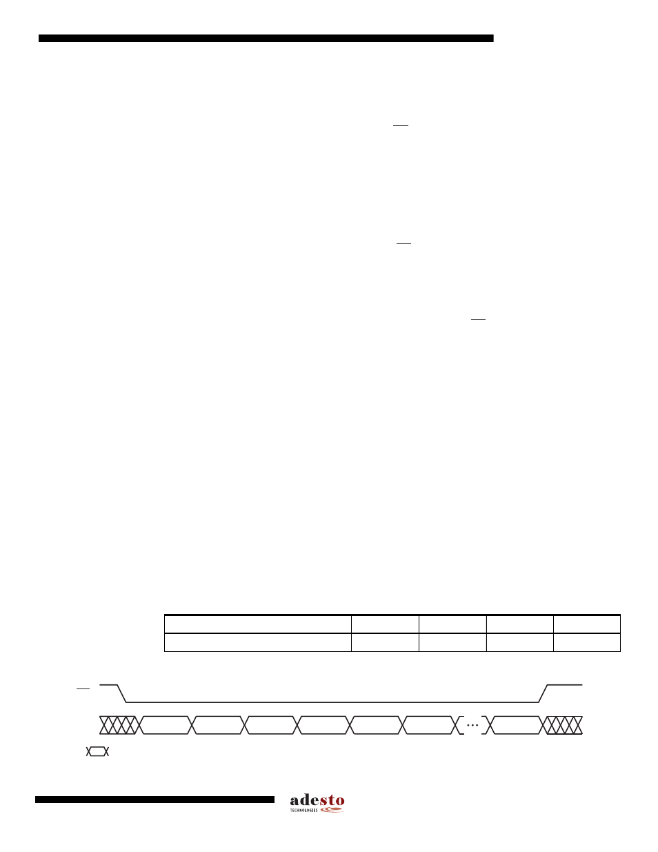
To program the Sector Protection Register, the CS pin must first be asserted and the appropri-
ate 4-byte opcode sequence must be clocked into the device via the SI pin. The 4-byte opcode
sequence must start with 3DH and be followed by 2AH, 7FH, and FCH. After the last bit of the
opcode sequence has been clocked into the device, the data for the contents of the Sector Pro-
tection Register must be clocked in. As described in
, the Sector Protection Register
contains four bytes of data, so four bytes must be clocked into the device. The first byte of data
corresponds to sector 0, the second byte corresponds to sector 1, the third byte corresponds to
sector 2, and the last byte of data corresponding to sector 3.
After the last data byte has been clocked in, the CS pin must be deasserted to initiate the inter-
nally self-timed program cycle. The programming of the Sector Protection Register should take
place in a time of t
P
, during which time the Status Register will indicate that the device is busy. If
the device is powered-down during the program cycle, then the contents of the Sector Protection
Register cannot be guaranteed.
If the proper number of data bytes is not clocked in before the CS pin is deasserted, then the
protection status of the sectors corresponding to the bytes not clocked in can not be guaranteed.
For example, if only the first two bytes are clocked in instead of the complete 4-bytes, then the
protection status of the last two sectors cannot be guaranteed. Furthermore, if more than four
bytes of data is clocked into the device, then the data will wrap back around to the beginning of
the register. For instance, if five bytes of data are clocked in, then the 5
th
byte will be stored at
byte location 0 of the Sector Protection Register.
If a value other than 00H or FFH is clocked into a byte location of the Sector Protection Register,
then the protection status of the sector corresponding to that byte location cannot be guaran-
teed. For example, if a value of 17H is clocked into byte location 2 of the Sector Protection
Register, then the protection status of sector 2 cannot be guaranteed.
The Sector Protection Register can be reprogrammed while the sector protection enabled or dis-
abled. Being able to reprogram the Sector Protection Register with the sector protection enabled
allows the user to temporarily disable the sector protection to an individual sector rather than
disabling sector protection completely.
The Program Sector Protection Register command utilizes the internal SRAM buffer for
processing. Therefore, the contents of the buffer will be altered from its previous state when this
command is issued.
Table 9-5.
Program Sector Protection Register Command
Figure 9-3.
Program Sector Protection Register
Command
Byte 1
Byte 2
Byte 3
Byte 4
Program Sector Protection Register
3DH
2AH
7FH
FCH
Data Byte
n
Opcode
Byte 1
Opcode
Byte 2
Opcode
Byte 3
Opcode
Byte 4
Data Byte
n + 1
Data Byte
n + 3
CS
Each transition
represents 8 bits
SI
