7 chip erase – Rainbow Electronics AT45DB011D User Manual
Page 10
10
3639J–DFLASH–11/2012
AT45DB011D
7.7
Chip Erase
The entire main memory can be erased at one time by using the Chip Erase command.
To execute the Chip Erase command, a 4-byte command sequence C7H, 94H, 80H and 9AH
must be clocked into the device. Since the entire memory array is to be erased, no address
bytes need to be clocked into the device, and any data clocked in after the opcode will be
ignored. After the last bit of the opcode sequence has been clocked in, the CS pin can be deas-
serted to start the erase process. The erase operation is internally self-timed and should take
place in a time of t
CE
. During this time, the Status Register will indicate that the device is busy.
The Chip Erase command will not affect sectors that are protected or locked down; the contents
of those sectors will remain unchanged. Only those sectors that are not protected or locked
down will be erased.
The WP pin can be asserted while the device is erasing, but protection will not be activated until
the internal erase cycle completes.
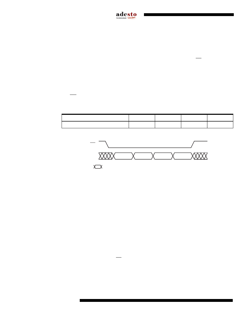
Table 7-3.
Chip Erase Command
Figure 7-1.
Chip Erase
7.8
Main Memory Page Program Through Buffer
This operation is a combination of the Buffer Write and Buffer to Main Memory Page Program
with Built-in Erase operations. Data is first clocked into the buffer from the input pin (SI) and then
programmed into a specified page in the main memory. To perform a main memory page pro-
gram through buffer for the DataFlash standard page size (264-bytes), a 1-byte opcode, 82H,
must first be clocked into the device, followed by three address bytes. The address bytes are
comprised of six don’t care bits, nine page address bits, (PA8 - PA0) that select the page in the
main memory where data is to be written, and nine buffer address bits (BFA8 - BFA0) that select
the first byte in the buffer to be written. To perform a main memory page program through buffer
for the binary page size (256-bytes), the opcode 82H must be clocked into the device followed
by three address bytes consisting of seven don’t care bits, nine page address bits (A16 - A8)
that specify the page in the main memory to be written, and eight buffer address bits (BFA7 -
BFA0) that selects the first byte in the buffer to be written. After all address bytes are clocked in,
the part will take data from the input pins and store it in the specified data buffer. If the end of the
buffer is reached, the device will wrap around back to the beginning of the buffer. When there is
a low-to-high transition on the CS pin, the part will first erase the selected page in main memory
to all 1s and then program the data stored in the buffer into that memory page. Both the erase
and the programming of the page are internally self-timed and should take place in a maximum
time of t
EP
. During this time, the status register will indicate that the part is busy.
Command
Byte 1
Byte 2
Byte 3
Byte 4
Chip Erase
C7H
94H
80H
9AH
Opcode
Byte 1
Opcode
Byte 2
Opcode
Byte 3
Opcode
Byte 4
CS
Each transition
represents 8 bits
SI