C-interface, digital potentiometers, Timing characteristics (continued) – Rainbow Electronics MAX5479 User Manual
Page 4
MAX5477/MAX5478/MAX5479
Dual, 256-Tap, Nonvolatile, I
2
C-Interface,
Digital Potentiometers
4
_______________________________________________________________________________________
Note 1:
All devices are production tested at T
A
= +25°C and are guaranteed by design and characterization for -40°C < T
A
< +85°C.
Note 2:
The DNL and INL are measured with the potentiometer configured as a voltage-divider with H_ = V
DD
and L_ = GND. The
wiper terminal is unloaded and measured with a high-input-impedance voltmeter.
Note 3:
The DNL and INL are measured with the potentiometer configured as a variable resistor. H_ is unconnected and L_ =
GND. For V
DD
= +5V, the wiper is driven with 400µA (MAX5477), 80µA (MAX5478), or 40µA (MAX5479). For V
DD
= +3V,
the wiper is driven with 200µA (MAX5477), 40µA (MAX5478), or 20µA (MAX5479).
Note 4:
The wiper resistance is measured using the source currents given in Note 3.
Note 5:
The devices draw current in excess of the specified supply current when the digital inputs are driven with voltages between
(V
DD
- 0.5V) and (GND + 0.5V). See Supply Current vs. Digital Input Voltage in the Typical Operating Characteristics.
Note 6:
Wiper at midscale with a 10pF load (DC measurement). L_ = GND, an AC source is applied to H_, and the W_ output is
measured. A 3dB bandwidth occurs when the AC W_/H_ value is 3dB lower than the DC W_/H_ value.
Note 7:
The programming current exists only during power-up and EEPROM writes.
Note 8:
The SCL clock period includes rise and fall times (t
R
= t
F
). All digital input signals are specified with t
R
= t
F
= 2ns and
timed from a voltage level of (V
IL
+ V
IH
) / 2.
Note 9:
Digital timing is guaranteed by design and characterization, and is not production tested.
Note 10: This is measured from the STOP pulse to the time it takes the output to reach 50% of the output step size (divider mode). It
is measured with a maximum external capacitive load of 10pF.
Note 11: An appropriate bus pullup resistance must be selected depending on board capacitance. Refer to the I
2
C-bus specifica-
tion document linked to this web address: www.semiconductors.philips.com/acrobat/literature/9398/39340011.pdf
Note 12: The idle time begins from the initiation of the STOP pulse.
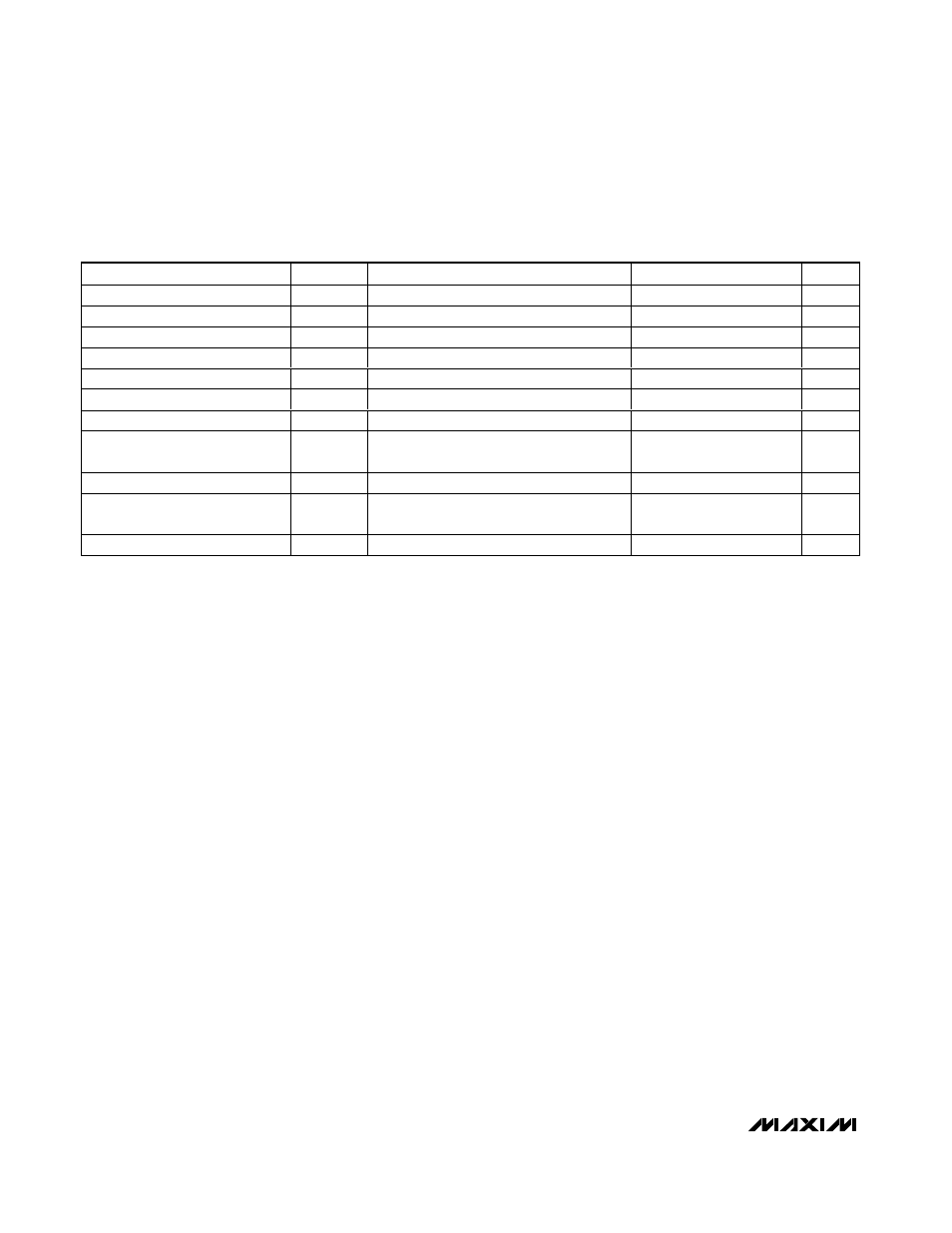
PARAMETER
SYMBOL
CONDITIONS
MIN
TYP
MAX
UNITS
SCL High Time
t
HIGH
0.6
µs
SCL Low Time
t
LOW
1.3
µs
Data Setup Time
t
SU:DAT
100
ns
Data Hold Time
t
HD:DAT
0
0.9
µs
SDA, SCL Rise Time
t
R
300
ns
SDA, SCL Fall Time
t
F
300
ns
Setup Time for STOP Condition
t
SU:STO
0.6
µs
Bus Free Time Between STOP
and START Condition
t
BUF
Minimum power-up rate = 0.2V/µs
1.3
µs
Pulse Width of Spike Suppressed
t
SP
50
ns
Capacitive Load for Each Bus
Line
C
B
(Note 11)
400
pF
Write NV Register Busy Time
(Note 12)
12
ms
TIMING CHARACTERISTICS (continued)
(V
DD
= +2.7V to +5.25V, H_ = V
DD
, L_ = GND, T
A
= -40°C to +85°C, unless otherwise noted. Typical values are at V
DD
= +5V,
T
A
= +25°C. See Figure 1.) (Notes 8 and 9)