C-interface, digital potentiometers, Table 1. slave addresses – Rainbow Electronics MAX5479 User Manual
Page 10
MAX5477/MAX5478/MAX5479
Dual, 256-Tap, Nonvolatile, I
2
C-Interface,
Digital Potentiometers
10
______________________________________________________________________________________
V
DD
. Connect WP to GND to allow write commands to
the EEPROM and to update the wiper position from
either the value in the EEPROM or directly from the I
2
C
interface. Connecting WP to GND increases the supply
current by 19.6µA (max).
Serial Addressing
The MAX5477/MAX5478/MAX5479 operate as slave
devices that send and receive data through an I
2
C-/
SMBus™-compatible 2-wire serial interface. The inter-
face uses a serial data access (SDA) line and a serial
clock line (SCL) to achieve bidirectional communication
between master(s) and slave(s). A master, typically a
microcontroller, initiates all data transfers to the
MAX5477/MAX5478/MAX5479, and generates the SCL
clock that synchronizes the data transfer (Figure 1).
The MAX5477/MAX5478/MAX5479 SDA line operates
as both an input and an open-drain output. The SDA
line requires a pullup resistor, typically 4.7k
Ω. The
MAX5477/MAX5478/MAX5479 SCL line operates only
as an input. The SCL line requires a pullup resistor (typ-
ically 4.7k
Ω) if there are multiple masters on the 2-wire
interface, or if the master in a single-master system has
an open-drain SCL output. SCL and SDA should not
exceed V
DD
in a mixed-voltage system, despite the
open-drain drivers.
Each transmission consists of a START (S) condition
(Figure 3) sent by a master, followed by the
MAX5477/MAX5478/MAX5479 7-bit slave address plus
the NOP/
W bit (Figure 4), 1 command byte and 1 data
byte, and finally a STOP (P) condition (Figure 3).
Start and Stop Conditions
Both SCL and SDA remain high when the interface is
not busy. A master controller signals the beginning of a
transmission with a START condition by transitioning
SDA from high to low while SCL is high. The master
controller issues a STOP condition by transitioning the
SDA from low to high while SCL is high, when it finishes
communicating with the slave. The bus is then free for
another transmission (Figure 3).
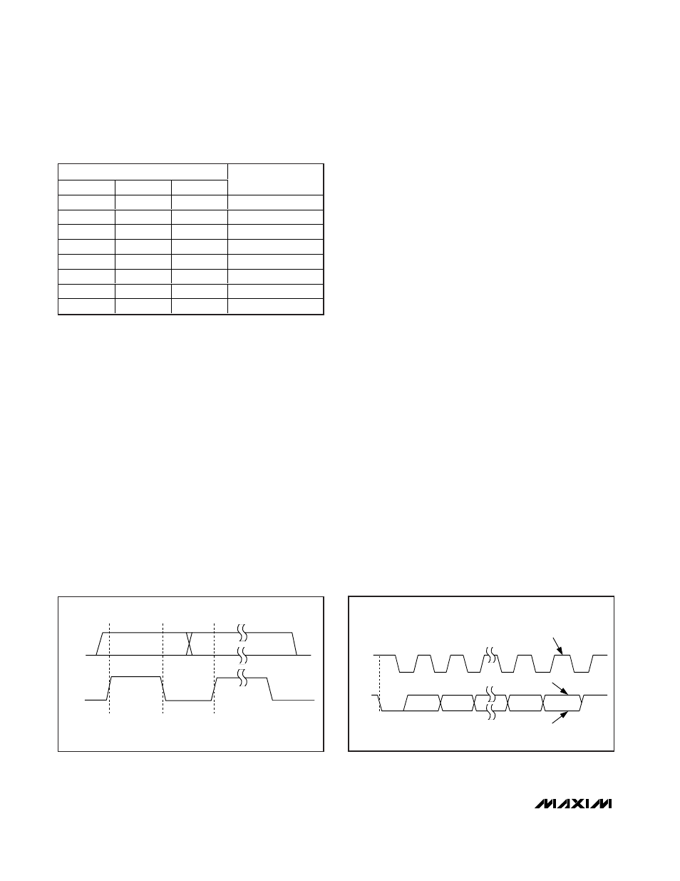
Bit Transfer
One data bit is transferred during each clock pulse.
The data on the SDA line must remain stable while SCL
is high (Figure 5).
Acknowledge
The acknowledge bit is a clocked 9th bit that the recipient
uses to handshake receipt of each byte of data (Figure
6). Thus, each byte transferred effectively requires 9 bits.
The master controller generates the 9th clock pulse, and
the recipient pulls down SDA during the acknowledge
clock pulse, so the SDA line remains stable low during
the high period of the clock pulse.
Slave Address
The MAX5477/MAX5478/MAX5479 have a 7-bit-long
slave address (Figure 4). The 8th bit following the 7-bit
ADDRESS INPUTS
A2
A1
A0
SLAVE ADDRESS
GND
GND
GND
0101000
GND
GND
V
DD
0101001
GND
V
DD
GND
0101010
GND
V
DD
V
DD
0101011
V
DD
GND
GND
0101100
V
DD
GND
V
DD
0101101
V
DD
V
DD
GND
0101110
V
DD
V
DD
V
DD
0101111
SDA
DATA STABLE,
DATA VALID
CHANGE OF
DATA ALLOWED
SCL
Figure 5. Bit Transfer
1
SCL
START
CONDITION
SDA
2
8
9
CLOCK PULSE FOR
ACKNOWLEDGMENT
ACKNOWLEDGE
NOT ACKNOWLEDGE
Figure 6. Acknowledge
SMBus is a trademark of Intel Corporation.
Table 1. Slave Addresses