Rainbow Electronics MAX7036 User Manual
Page 2
MAX7036
300MHz to 450MHz ASK Receiver
with Internal IF Filter
2
_______________________________________________________________________________________
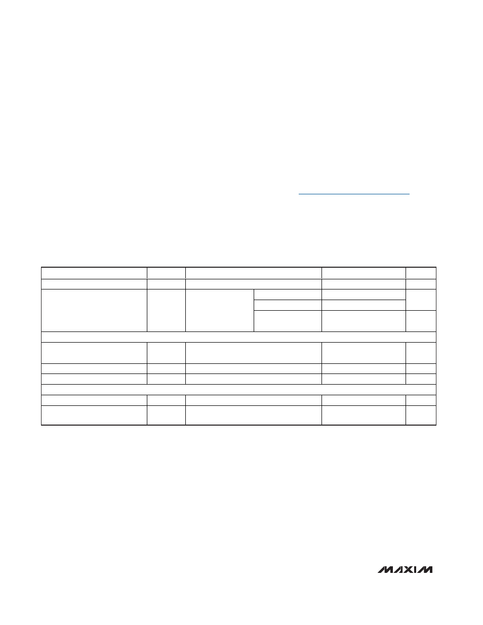
ABSOLUTE MAXIMUM RATINGS
3.3V DC ELECTRICAL CHARACTERISTICS
(
Typical Application Circuit, 50
Ω system impedance, V
AVDD
= V
DVDD
= V
DD
= 3.0V to 3.6V, f
RF
= 300MHz to 450MHz, T
A
= -40°C to
+105°C, unless otherwise noted. Typical values are at V
AVDD
= V
DVDD
= V
DD
= 3.3V, T
A
= +25°C, unless otherwise noted.) (100%
tested at T
A
= +105°C.)
Stresses beyond those listed under “Absolute Maximum Ratings” may cause permanent damage to the device. These are stress ratings only, and functional
operation of the device at these or any other conditions beyond those indicated in the operational sections of the specifications is not implied. Exposure to
absolute maximum rating conditions for extended periods may affect device reliability.
V
DD
to GND ...........................................................-0.3V to +6.0V
AVDD to GND........................................................-0.3V to +4.0V
DVDD to GND........................................................-0.3V to +4.0V
ENABLE to GND.........................................-0.3V to (V
DD
+ 0.3V)
LNAIN to GND .......................................................-0.3V to +1.2V
All Other Pins to GND.............................-0.3V to (V
DVDD
+ 0.3V)
Continuous Power Dissipation (T
A
= +70°C)
20-Pin TQFN (derate 20.8mW/°C above +70°C) ....1666.7mW
Junction-to-Case Thermal Resistance (
θ
JA
) (Note 1)
20-Pin TQFN...................................................................2°C/W
Junction-to-Ambient Thermal Resistance (
θ
JA
) (Note 1)
20-Pin TQFN.................................................................48°C/W
Operating Temperature Range .........................-40°C to +105°C
Junction Temperature ......................................................+150°C
Storage Temperature Range .............................-65°C to +150°C
Lead Temperature (soldering, 10s) .................................+300°C
PARAMETER
SYMBOL
CONDITIONS
MIN
TYP
MAX
UNITS
Supply Voltage
V
DD
V
AVDD
= V
DVDD
= V
DD
3.0
3.3
3.6
V
f
RF
= 315MHz
5.3
6.7
f
RF
= 433MHz
5.8
7.3
mA
Supply Current
I
IN
T
A
< +105°C
Deep-sleep mode,
V
ENABLE
= 0
1
2.7
µA
DIGITAL INPUT (ENABLE)
Input High Voltage
V
IH
V
AVDD
= V
DVDD
= V
DD
V
DD
-
0.4
V
Input Low Voltage
V
IL
V
AVDD
= V
DVDD
= V
DD
0.4
V
Input Current
I
ENABLE
0
≤ V
ENABLE
≤ V
DD
20
µA
DIGITAL OUTPUT (DATAOUT)
Output Low Voltage
V
OL
I
SINK
= 100µA
0.4
V
Output High Voltage
V
OH
I
SOURCE
= 100µA
V
DD
-
0.4
V
Note 1: Package thermal resistances were obtained using the method described in JEDEC specification JESD51-7, using a single-
layer board. For detailed information on package thermal considerations, go to
www.maxim-ic.com/thermal-tutorial
.