Electrical characteristics (continued) – Rainbow Electronics MAX8720 User Manual
Page 6
MAX8720
Dynamically Adjustable 6-Bit VID
Step-Down Controller
6
_______________________________________________________________________________________
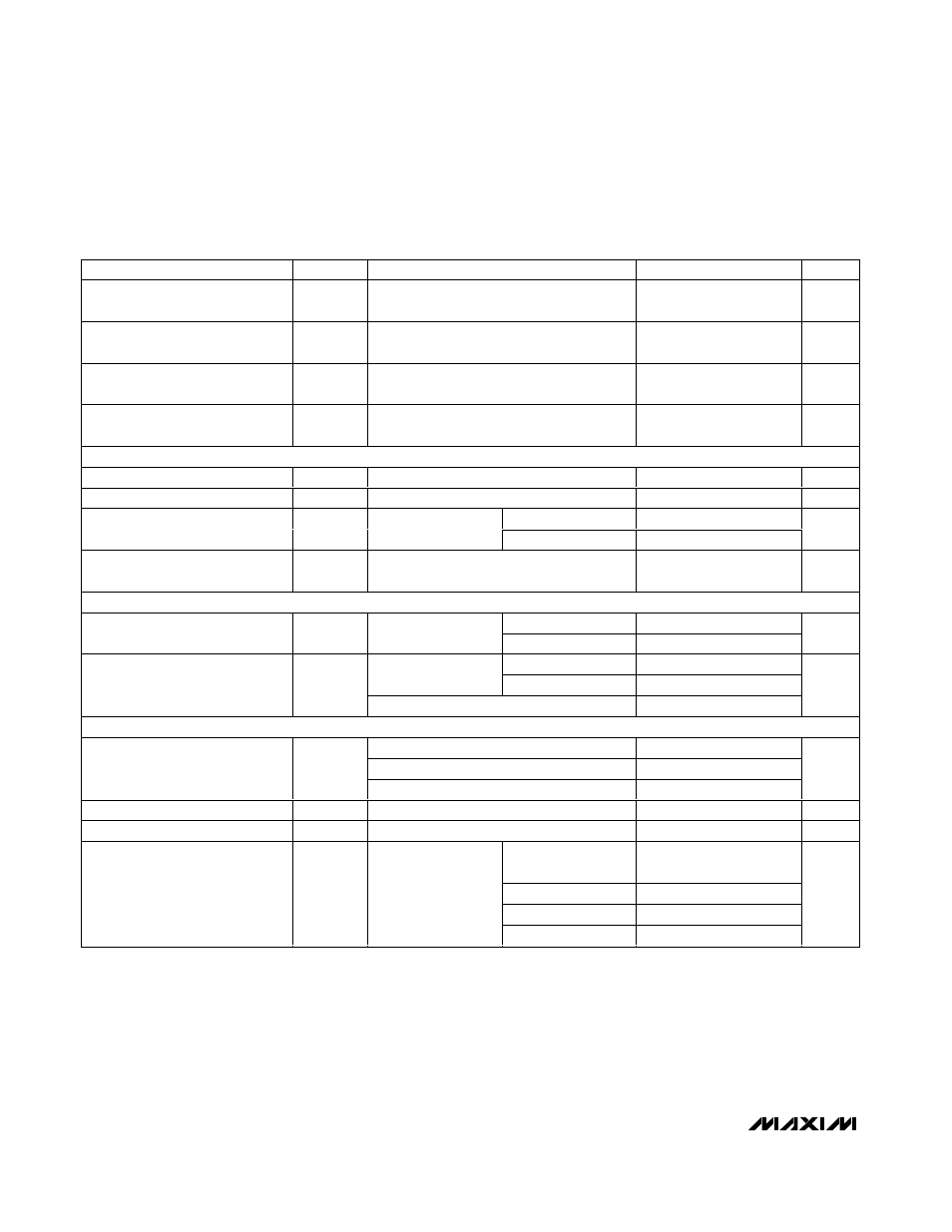
ELECTRICAL CHARACTERISTICS (continued)
(Circuit of Figure 1, V+ =15V, SHDN = SKIP = V
DD
= V
CC
= +5V, V
OUT
= 1.25V, T
A
= -40°C to +85°C, unless otherwise noted.
Typical values are at T
A
= +25°C.) (Note 4)
PARAMETER
SYMBOL
CONDITIONS
MIN
TYP
MAX
UNITS
Output Overvoltage Trip
Threshold
2.20
2.30
V
Output Undervoltage-Protection
Trip Threshold
With respect to unloaded output voltage
65
75
%
PGOOD Lower Trip Threshold
Measured at FB with respect to unloaded
output voltage, hysteresis = 1%
-17.5
-12.5
%
PGOOD Upper Trip Threshold
Measured at FB with respect to unloaded
output voltage, hysteresis = 1%
+12.5
+17.5
%
CURRENT LIMIT
ILIM Adjustment Range
0.5
V
REF
V
Current-Limit Threshold (Fixed)
V
LIMIT
V
PGND
- V
LX
, ILIM = V
CC
80
115
mV
V
ILIM
= 2.00V
160
240
Current-Limit Threshold
(Adjustable)
V
LIMIT
V
PGND
- V
LX
V
ILIM
= 0.50V
33
65
mV
Current-Limit Threshold
(Negative)
V
NEG
V
LX
- V
PGND
, SKIP = ILIM = V
CC
-140
-85
mV
GATE DRIVERS
QSOP package
3.5
DH Gate-Driver On-Resistance
(Note 3)
R
DH
BST-LX forced to 5V
TQFN package
4.5
Ω
QSOP package
3.5
DL, high state
TQFN package
4.0
DL Gate-Driver On-Resistance
(Note 3)
R
DL
DL, low state
1.0
Ω
INPUTS AND OUTPUTS
Logic high
2.4
Logic low
0.4
SHDN Input Level
V
SHDN
No-fault mode
12
15
V
Logic Input High Voltage
V
IH
D0–D5, SKIP, SUS
2.4
V
Logic Input Low Voltage
V
IL
D0–D5, SKIP, SUS
0.8
V
High
V
CC
-
0.2
Open
3.15
3.85
REF
1.65
2.35
Four-Level Input Logic
TON, S0, S1
GND
0.5
V
Note 2: On-time specifications are measured from 50% to 50% at the DH pin, with LX forced to 0, BST forced to 5V, and a 500pF
capacitor from DH to LX to simulate external MOSFET gate capacitance. Actual in-circuit times may be different due to
MOSFET switching speeds.
Note 3: Production testing limitations due to package handling require relaxed maximum on-resistance specifications for the thin
QFN package. The QSOP and thin QFN package contain the same die, and the thin QFN package imposes no additional
resistance in the circuit.
Note 4: Specifications to -40°C are guaranteed by design, not production tested.