Rainbow Electronics MAX8720 User Manual
Page 17
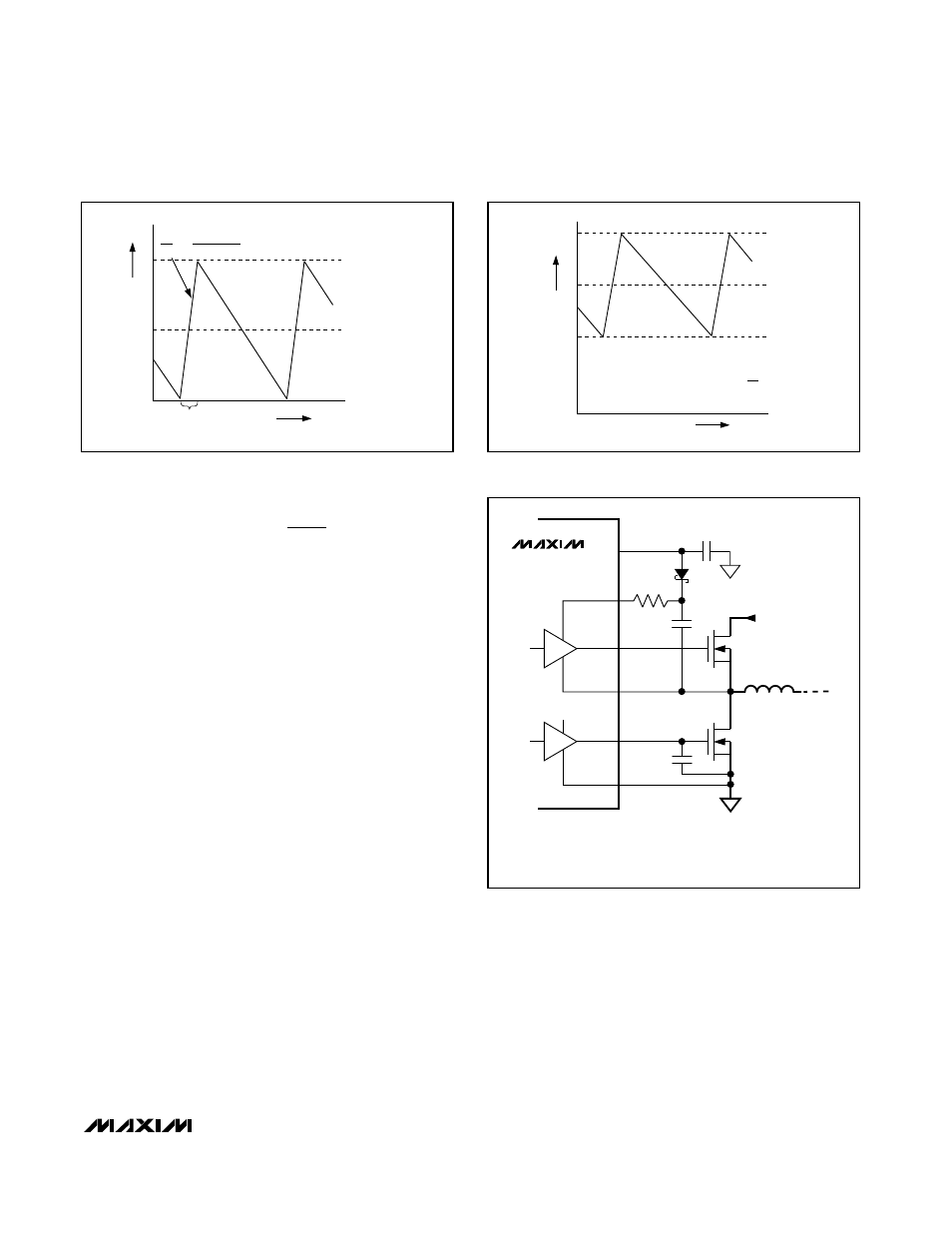
Lot-to-lot variation of the threshold voltage can cause
problems in marginal designs. Typically, adding
4700pF between DL and power ground (C
NL
in Figure
5), close to the low-side MOSFETs, greatly reduces
coupling. Do not exceed 22nF of total gate capacitance
to prevent excessive turn-off delays.
Alternatively, shoot-through currents may be caused by
a combination of fast high-side MOSFETs and slow low-
side MOSFETs. If the turn-off delay time of the low-side
MOSFET is too long, the high-side MOSFETs can turn
on before the low-side MOSFETs have actually turned
off. Adding a resistor less than 5
Ω in series with BST
slows down the high-side MOSFETs’ turn-on time, elimi-
nating the shoot-through currents without degrading
the turn-off time (R
BST
in Figure 5). Slowing down the
high-side MOSFETs also reduces the LX node rise
time, thereby reducing EMI and high-frequency cou-
pling responsible for switching noise.
V
CC
POR and UVLO
Power-on reset (POR) occurs when V
CC
rises above
approximately 2V, resetting the fault latch and prepar-
ing the PWM for operation. V
CC
undervoltage-lockout
(UVLO) circuitry inhibits switching, forces PGOOD low,
and forces the DL gate driver low. When V
CC
rises
above 4.2V, the DAC inputs are sampled and the out-
put voltage begins to slew to the DAC setting.
If V
CC
drops low enough to trip the UVLO comparator, it
is assumed that there is not enough supply voltage to
make valid decisions. The MAX8720 immediately forces
both DH and DL low. The output discharges to 0V at a
rate dependent on the load and the total output capaci-
tance. This prevents negative output voltages, eliminat-
ing the need for a Schottky diode to GND at the output.
For automatic startup, the battery voltage should be
present before V
CC
. If the MAX8720 attempts to bring
the output into regulation without the battery voltage
present, the fault latch trips. The SHDN pin can be tog-
gled to reset the fault latch.
V
V
C
C
GS TH
IN
RSS
ISS
(
)
>
MAX8720
Dynamically Adjustable 6-Bit VID
Step-Down Controller
______________________________________________________________________________________
17
INDUCTOR CURRENT
I
LOAD
= I
PEAK
/ 2
ON-TIME
0
TIME
I
PEAK
L
V
IN
- V
OUT
∆I
∆t
=
Figure 3. Pulse-Skipping/Discontinuous Crossover Point
INDUCTOR CURRENT
I
LIMIT
I
LOAD
0
TIME
I
PEAK
I
LIM(VAL)
= I
LOAD(MAX)
1-
LIR
2
(
)
Figure 4. Valley Current-Limit Threshold
MAX8720
V
DD
BST
DH
LX
(R
BST
)*
(C
NL
)*
D
BST
C
BST
C
BYP
INPUT (V
IN
)
N
H
L
V
DD
DL
PGND
N
L
(R
BST
)* OPTIONAL—THE RESISTOR LOWERS EMI BY DECREASING
THE SWITCHING-NODE RISE TIME.
(C
NL
)* OPTIONAL—THE CAPACITOR REDUCES LX TO DL CAPACITIVE
COUPLING THAT CAN CAUSE SHOOT-THROUGH CURRENTS.
Figure 5. Reducing the Switching-Node Rise Time