Chip information, Pin configurations, Layout procedure – Rainbow Electronics MAX8720 User Manual
Page 29
Layout Procedure
1) Place the power components first, with ground ter-
minals adjacent (NL source, C
IN
, C
OUT
, and DL
anode). If possible, make all these connections on
the top layer with wide, copper-filled areas.
2) Mount the controller IC adjacent to the low-side
MOSFET, preferably on the back side opposite NL
and NH to keep LX, GND, DH, and the DL gate-drive
lines short and wide. The DL and DH_ gate traces
must be short and wide (50 to 100 mils wide if the
MOSFET is 1in from the controller IC) to keep the dri-
ver impedance low and for proper adaptive dead-
time sensing.
3) Group the gate-drive components (BST diode and
capacitor, V
DD
bypass capacitor) together near the
controller IC.
4) Make the DC-DC controller ground connections as
shown in Figures 1 and 12. This diagram can be
viewed as having two separate ground planes:
power ground, where all the high-power compo-
nents go, and an analog ground plane for sensitive
analog components. The analog ground plane and
power ground plane must meet only at a single point
directly at the IC.
5) Connect the output power planes directly to the out-
put filter capacitor positive and negative terminals
with multiple vias. Place the entire DC-DC converter
circuit as close to the load as is practical.
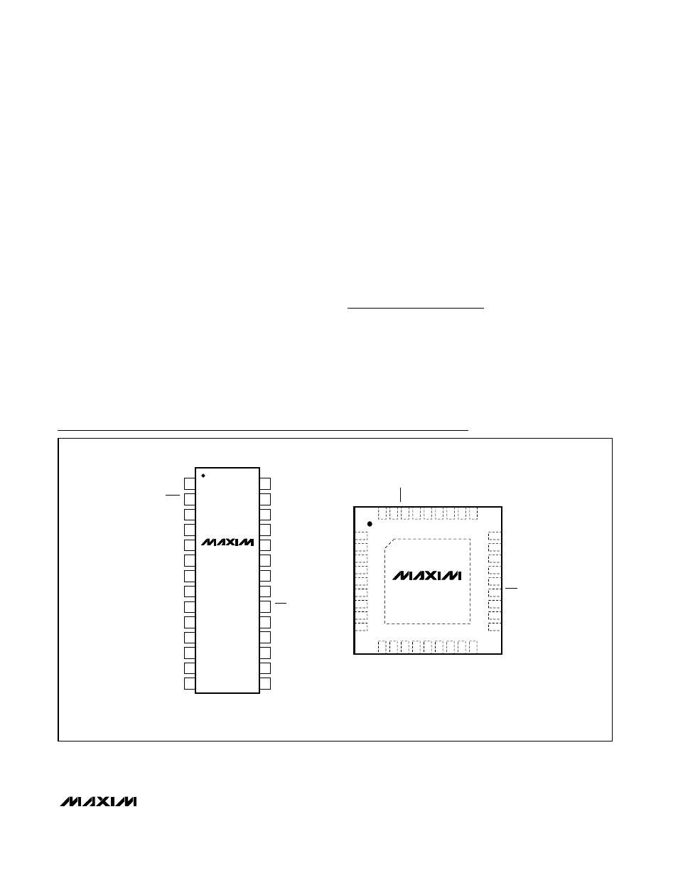
Chip Information
TRANSISTOR COUNT: 7190
PROCESS: BiCMOS
MAX8720
Dynamically Adjustable 6-Bit VID
Step-Down Controller
______________________________________________________________________________________
29
28
27
26
25
24
23
22
21
20
19
18
17
16
15
1
2
3
4
5
6
7
8
9
10
11
12
13
14
DH
LX
BST
D1
D2
D3
GND
D4
D5
SKIP
D0
SUS
V
DD
DL
PGOOD
GNDS
ILIM
REF
TON
V
CC
S1
S0
CC
FBS
FB
TIME
SHDN
V+
QSOP
TOP VIEW
MAX8720EEI
D1
D2
D4
D5
SUS
V
DD
SKIP
D0
D3
CC
S0
S1
V
CC
TON
REF
FB
1
2
3
4
5
6
7
8
9
36 35 34 33 32 31 30 29 28
10 11 12 13 14 15 16 17 18
27
26
25
24
23
22
21
20
19
PGND
PGND
DL
N.C.
AGND
PGOOD
GNDS
ILIM
TIME
SHDN
V+
DH
LX
N.C.
BST
N.C.
N.C.
THIN QFN
6mm x 6mm
MAX8720ETX
N.C.
DL
FBS
Pin Configurations