Max8720 – Rainbow Electronics MAX8720 User Manual
Page 28
MAX8720
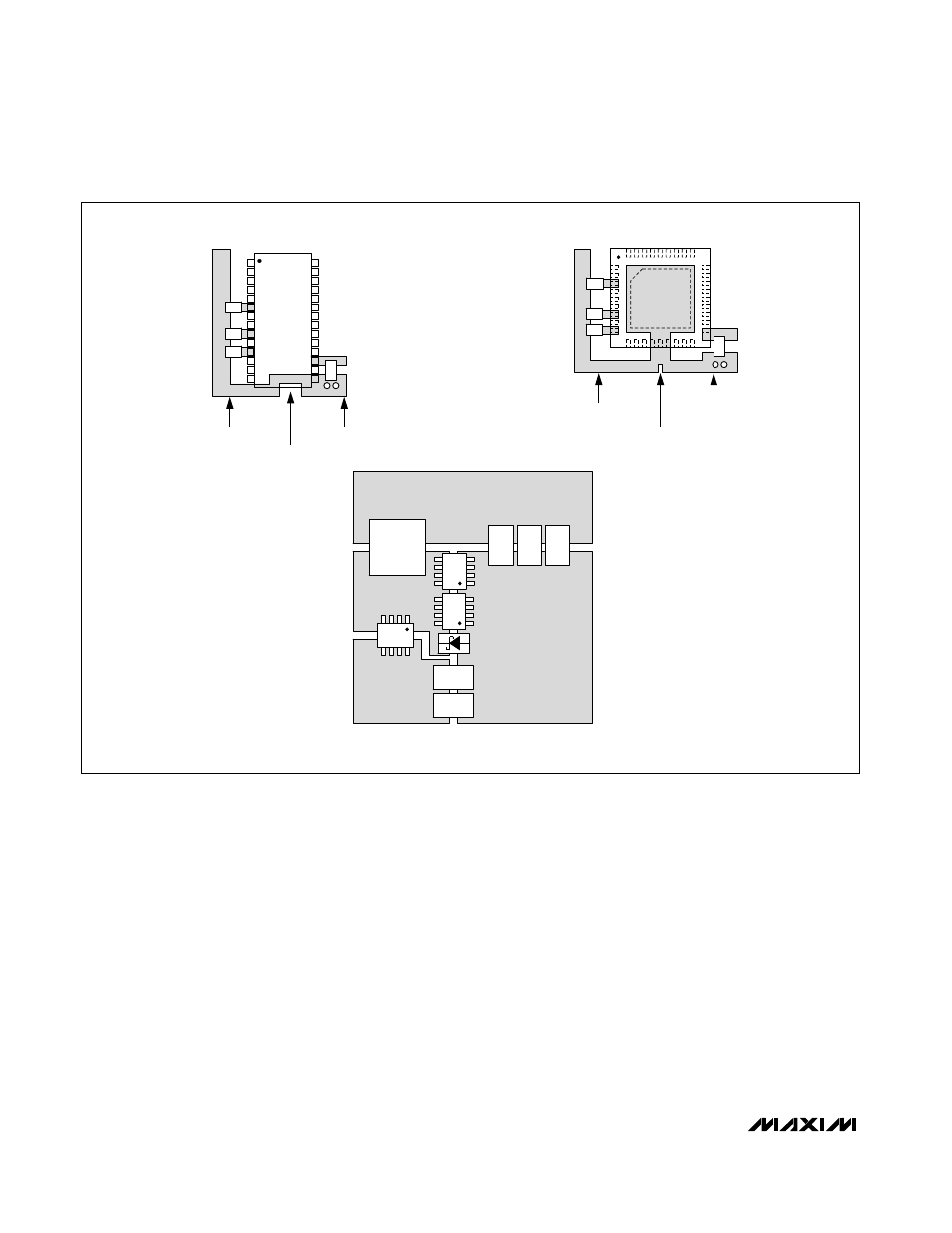
PC Board Layout Guidelines
Careful PC board layout is critical to achieving low
switching losses and clean, stable operation. The
switching power stage requires particular attention
(Figure 12). If possible, mount all of the power compo-
nents on the top side of the board, with their ground
terminals flush against one another. Follow these guide-
lines for good PC board layout:
• Keep the high-current paths short, especially at the
ground terminals. This practice is essential for sta-
ble, jitter-free operation.
• Keep the power traces and load connections short.
This practice is essential for high efficiency. Using
thick copper PC boards (2oz vs. 1oz) can enhance
full-load efficiency by 1% or more. Correctly routing
PC board traces is a difficult task that must be
approached in terms of fractions of centimeters,
where a single milliohm of excess trace resistance
causes a measurable efficiency penalty.
• When trade-offs in trace lengths must be made, it is
preferable to allow the inductor charging path to be
made longer than the discharge path. For example,
it is better to allow some extra distance between the
input capacitors and the high-side MOSFET than to
allow distance between the inductor and the low-
side MOSFET or between the inductor and the out-
put filter capacitor.
• Route high-speed switching nodes (BST, LX, DH, and
DL) away from sensitive analog areas (REF, FB).
Dynamically Adjustable 6-Bit VID
Step-Down Controller
28
______________________________________________________________________________________
INDUCTOR
INPUT
GROUND
OUTPUT
C
IN
C
IN
QSOP LAYOUT EXAMPLE
CONNECT AGND
AND PGND TO THE
CONTROLLER AT
ONE POINT ONLY
AS SHOWN
ANALOG
GROUND
POWER
GROUND
QFN LAYOUT EXAMPLE
CONNECT AGND
AND PGND TO THE
CONTROLLER AT
ONE POINT ONLY
AS SHOWN
ANALOG
GROUND
POWER
GROUND
V
CC
CC
REF
V
DD
C
OUT
C
OUT
C
OUT
POWER STAGE LAYOUT EXAMPLE
Figure 12. PC Board Layout Example