T5744, Analog signal processing, If amplifier – Rainbow Electronics T5744 User Manual
Page 6: Rssi amplifier, Pin rssi
6
T5744
4521A–RKE–02/02
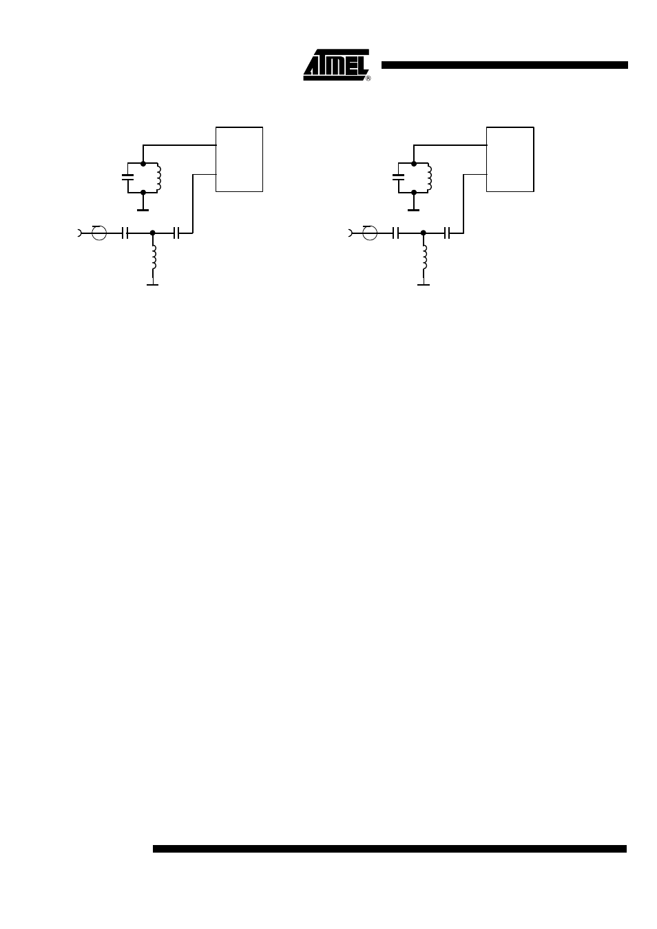
Figure 6. Input Matching Network without SAW Filter
Please note that for all coupling conditions (see Figure 5 and Figure 6), the bond wire
inductivity of the LNA ground is compensated. C3 forms a series resonance circuit
together with the bond wire. L = 25 nH is a feed inductor to establish a DC path. Its value
is not critical but must be large enough not to detune the series resonance circuit. For
cost reduction, this inductor can be easily printed on the PCB. This configuration
improves the sensitivity of the receiver by about 1 dB to 2 dB.
Analog Signal Processing
IF Amplifier
The signals coming from the RF front end are filtered by the fully integrated 4th-order IF
filter. The IF center frequency is f
IF
= 1 MHz for applications where f
RF
= 315 MHz or
f
RF
= 433.92 MHz is used. For other RF input frequencies, refer to Table 1 to determine
the center frequency.
The receiver T5744 employs an IF bandwidth of B
IF
= 600 kHz and can be used
together with the U2741B in ASK mode.
RSSI Amplifier
The subsequent RSSI amplifier enhances the output signal of the IF amplifier before it is
fed into the demodulator. The dynamic range of this amplifier is DRRSSI = 60 dB. If the
RSSI amplifier is operated within its linear range, the best S/N ratio is maintained. If the
dynamic range is exceeded by the transmitter signal, the S/N ratio is defined by the ratio
of the maximum RSSI output voltage and the RSSI output voltage due to a disturber.
The dynamic range of the RSSI amplifier is exceeded if the RF input signal is about
60 dB higher compared to the RF input signal at full sensitivity.
Pin RSSI
The output voltage of the RSSI amplifier (VRSSI) is available at Pin RSSI. Using the
RSSI output signal, the signal strength of different transmitters can be distinguished.
The usable input power range P
Ref
is -100 dBm to -55 dBm.
Since different RF input networks may exhibit slightly different values for the LNA gain,
the sensitivity values given in the electrical characteristics refer to a specific input
matching. This matching is illustrated in Figure 6 and exhibits the best possible
sensitivity.
T5744
C3
15p
25n
100p
3.3p
TOKO LL2012
F22NJ
22n
8
9
RF
IN
f
RF
= 433.92 MHz
LNAGND
LNA_IN
T5744
C3
33p
25n
100p
3.3p
TOKO LL2012
F39NJ
39n
8
9
f
RF
= 315 MHz
LNAGND
LNA_IN
RF
IN