T5744, Rf front end – Rainbow Electronics T5744 User Manual
Page 3
3
T5744
4521A–RKE–02/02
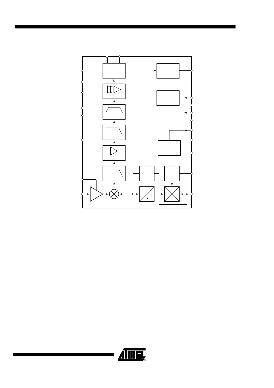
Figure 3. Block Diagram
RF Front End
The RF front end of the receiver is a heterodyne configuration that converts the input
signal into a 1-MHz IF signal. According to Figure 3, the front end consists of an LNA
(Low-Noise Amplifier), LO (Local Oscillator), a mixer and RF amplifier.
The LO generates the carrier frequency for the mixer via a PLL synthesizer. The XTO
(crystal oscillator) generates the reference frequency f
XTO
. The VCO (Voltage-Controlled
Oscillator) generates the drive voltage frequency f
LO
for the mixer. f
LO
is dependent on
the voltage at Pin LF. f
LO
is divided by factor 64. The divided frequency is compared to
f
XTO
by the phase frequency detector. The current output of the phase frequency detec-
tor is connected to a passive loop filter and thereby generates the control voltage VLF
for the VCO. By means of that configuration, VLF is controlled in a way that f
LO
/64 is
equal to f
XTO
. If f
LO
is determined, f
XTO
can be calculated using the following formula:
f
XTO
= f
LO
/64
The XTO is a one-pin oscillator that operates at the series resonance of the quartz crys-
tal. According to Figure 4, the crystal should be connected to GND via a capacitor CL.
The value of that capacitor is recommended by the crystal supplier. The value of CL
should be optimized for the individual board layout to achieve the exact value of f
XTO
and
hereby of f
LO
. When designing the system in terms of receiving bandwidth, the accuracy
of the crystal and the XTO must be considered.
ASK-
Demodulator
and data filter
RSSI IF Amp
IF Amp
4. Order
LPF
3 MHz
LPF
3 MHz
Dem_out
RSSI
Standby logic
VCO
XTO
64
f
CDEM
AVCC
RSSI
AGND
DGND
MIXVCC
LNAGND
LNA_IN
DATA
ENABLE
TEST
MODE
LFGND
LFVCC
XTO
LF
DVCC
LNA
Data interface
Test
BR_0
BR_1