Rainbow Electronics MAX7057 User Manual
Page 2
MAX7057
300MHz to 450MHz Frequency-Programmable
ASK/FSK Transmitter
2
_______________________________________________________________________________________
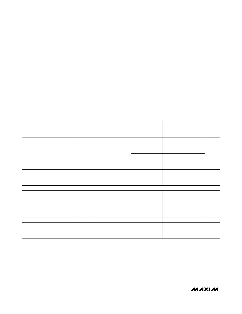
ABSOLUTE MAXIMUM RATINGS
DC ELECTRICAL CHARACTERISTICS
(
Typical Application Circuit, 50Ω system impedance, tuned for 315MHz to 433.92MHz operation, AVDD = DVDD = PAVDD = +2.1V to
+3.6V, f
RF
= 300MHz to 450MHz, f
CRYSTAL
= 16MHz, T
A
= -40°C to +125°C, unless otherwise noted. Typical values are at AVDD =
DVDD = PAVDD = +2.7V, T
A
= +25°C, unless otherwise noted. All min and max values are 100% tested at T
A
= +125°C, and guaran-
teed by design and characterization over temperature, unless otherwise noted.)
Stresses beyond those listed under “Absolute Maximum Ratings” may cause permanent damage to the device. These are stress ratings only, and functional
operation of the device at these or any other conditions beyond those indicated in the operational sections of the specifications is not implied. Exposure to
absolute maximum rating conditions for extended periods may affect device reliability.
Supply Voltage, PAVDD, AVDD, DVDD to AGND,
DGND, PAGND ...................................................-0.3V to +4.0V
All Other Pins..................................._GND - 0.3V to _V
DD
+ 0.3V
Continuous Power Dissipation (T
A
= +70°C)
16-Pin SO (derate 8.7mW/°C above +70°C)...............695.7mW
Operating Temperature .....................................-40°C to +125°C
Storage Temperature Range .............................-65°C to +150°C
Lead Temperature (soldering, 10s) .................................+300°C
PARAMETER
SYMBOL
CONDITIONS
MIN
TYP
MAX
UNITS
Supply Voltage
V
DD
PAVDD, AVDD, and DVDD connected to
power supply, V
DD
2.1
2.7
3.6
V
f
RF
= 315MHz
3.9
6.5
PA off, V
DIN
at 0%
duty cycle (ASK)
f
RF
= 433.92MHz
4.5
7.5
f
RF
= 315MHz
8.1
15.1
V
D IN
at 50% d uty cycl e
( AS K) ( N otes 1, 2, 3)
f
RF
= 433.92MHz
8.5
15.0
f
RF
= 315MHz
12.2
23.7
Supply Current
I
DD
V
DIN
at 100% duty
cycle (FSK) (Note 1)
f
RF
= 433.92MHz
12.4
22.4
mA
T
A
= + 25°C ( N ote 3)
0.8
T
A
< + 85°C ( N ote 3)
1
6.4
Standby Current
I
STDBY
V
ENABLE
< V
IL
T
A
< +125°C
6.2
20.1
μA
DIGITAL I/O
Input High Threshold
V
IH
0.9 x
DV
DD
V
Input Low Threshold
V
IL
0.1 x
DV
DD
V
Input Pulldown Sink Current
13
μA
Input Pullup Source Current
9
μA
Output-Voltage High
V
OH
I
SINK
= 500μA (GPO)
V
DD
-
0.37
V
Output-Voltage Low
V
OL
I
SOURCE
= 500μA (GPO)
0.36
V