Max6900 i, C-compatible rtc in a tdfn, Ac electrical characteristics (continued) – Rainbow Electronics MAX6900 User Manual
Page 3
MAX6900
I
2
C-Compatible RTC in a TDFN
_______________________________________________________________________________________
3
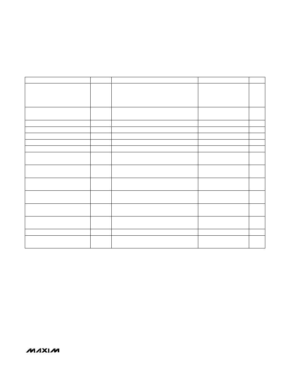
AC ELECTRICAL CHARACTERISTICS (continued)
(V
CC
= +2.0V to +5.5V, T
A
= T
MIN
to T
MAX
, unless otherwise noted. Typical values are at V
CC
= +3.3V, T
A
= +25°C.) (Notes 1, 6)
PARAMETER
SYMBOL
CONDITIONS
MIN
TYP
MAX
UNITS
Hold Time After (Repeated)
START Condition (After this
Period, the First Clock Is
Generated)
t
HD:STA
0.6
µs
Repeated START Condition
Setup Time
t
SU:STA
0.6
µs
STOP Condition Setup Time
t
SU:STO
0.6
µs
Data Hold Time (Note 7)
t
HD:DAT
0
0.9
µs
Data Setup Time
t
SU:DAT
100
ns
SCL Low Period
t
LOW
1.3
µs
SCL High Period
t
HIGH
0.6
µs
Minimum SCL/SDA Rise Time
(Note 8)
t
r
20 +
0.1C
B
ns
Maximum SCL/SDA Rise Time
(Note 8)
t
r
300
ns
Minimum SCL/SDA Fall Time
(Receiving) (Notes 8, 9)
t
f
20 +
0.1C
B
ns
Maximum SCL/SDA Fall Time
(Receiving) (Notes 8, 9)
t
f
300
ns
Minimum SDA Fall Time
(Transmitting) (Notes 8, 9)
t
f
20 +
0.1C
B
ns
Maximum SDA Fall Time
(Transmitting) (Notes 8, 9)
t
f
250
ns
Pulse Width of Spike Suppressed
t
SP
50
ns
Capacitive Load for Each
Bus Line
C
B
400
pF
Note 1: All parameters are 100% tested at T
A
= +25°C. Limits over temperature are guaranteed by design and not production tested.
Note 2: I
CC
is specified with SCL = 400kHz and SDA = 400kHz.
Note 3: I
TK
is specified with SCL = Logic High (4.7k
Ω pullup resistor) and SDA = Logic High (4.7kΩ pullup resistor);
I
2
C-compatible bus inactive.
Note 4: MAX6900 I/O pins do not obstruct the SDA and SCL lines if V
CC
is switched off.
Note 5: Guaranteed by design. Not subject to production testing.
Note 6: All values referred to V
IH min
and V
IL max
levels.
Note 7: The MAX6900 internally provides a hold time of at least 300ns for the SDA signal (referred to the V
IH min
of the SCL signal)
in order to bridge the undefined region of the falling edge of SCL.
Note 8: C
B
= total capacitance of one bus line in pF.
Note 9: The maximum t
f
for the SDA and SCL bus lines is specified at 300ns. The maximum fall time for the SDA output stage t
f
is
specified at 250ns. This allows series protection resistors to be connected between the SDA/SCL pins and the SDA/SCL
bus lines without exceeding the maximum specified t
f
.