Detailed description, Pin description – Rainbow Electronics MAX19997A User Manual
Page 29
MAX19997A
Dual, SiGe High-Linearity, 1800MHz to 2900MHz
Downconversion Mixer with LO Buffer
______________________________________________________________________________________
29
Detailed Description
The MAX19997A dual, downconversion mixer provides
high linearity and low noise figure for a multitude of
1800MHz to 2900MHz base-station applications. The
device fully supports both low-side and high-side LO
injection architectures for the 2300MHz to 2900MHz
WiMAX, LTE, WCS, and MMDS bands. WCDMA,
cdma2000, and PCS1900 applications utilizing high-
side LO injection architectures are also supported by
adding one additional tuning element (a shunt inductor)
on each RF port.
The MAX19997A operates over an LO range of
1950MHz to 3400MHz and an IF range of 50MHz to
500MHz. Integrated baluns and matching circuitry
allow 50
Ω single-ended interfaces to the RF and LO
ports. The integrated LO buffer provides a high drive
level to the mixer core, reducing the LO drive required
at the MAX19997A’s input to a range of -3dBm to
+3dBm. The IF port incorporates a differential output,
which is ideal for providing enhanced 2RF-2LO (low-
side injection) and 2LO-2RF (high-side injection) perfor-
mance.
RF Input and Balun
The MAX19997A’s two RF inputs (RFMAIN and RFDIV)
provide a 50
Ω match when combined with a series DC-
blocking capacitor. This DC-blocking capacitor is
required as the input is internally DC shorted to ground
through each channel’s on-chip balun. When using a
22pF DC-blocking capacitor, the RF port input return
loss is typically 15dB over the RF frequency range of
2600MHz to 2900MHz.
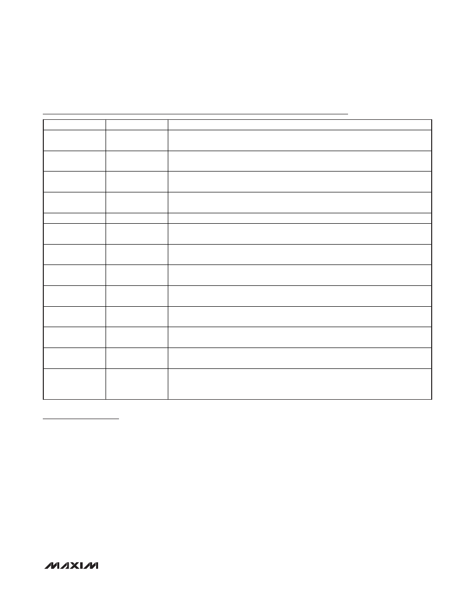
Pin Description
PIN
NAME
FUNCTION
1
RFMAIN
Main Channel RF Input. Internally matched to 50
Ω. Requires an input DC-blocking
capacitor.
2, 5, 6, 8, 12, 15,
18, 23, 28, 31, 34
GND
Ground. Not internally connected. Ground these pins or leave unconnected.
3, 7, 20, 22, 24–27
GND
Ground. Internally connected to the exposed pad. Connect all ground pins and the
exposed pad (EP) together.
4, 10, 16, 21, 30,
36
V
CC
Power Supply. Connect bypass capacitors as close as possible to the pin (see the
Typical Application Circuit).
9
RFDIV
Diversity Channel RF Input. Internal matched to 50
Ω. Requires a DC-blocking capacitor.
11
IFD_SET
IF Diversity Amplifier Bias Control. Connect a resistor from this pin to ground to set the
bias current for the diversity IF amplifier.
13, 14
IFD+, IFD-
Diversity Mixer Differential IF Output. Connect pullup inductors from each of these pins
to V
CC
(see the Typical Application Circuit).
17
LO_ADJ_D
LO Diversity Amplifier Bias Control. Connect a resistor from this pin to ground to set the
bias current for the diversity LO amplifier.
19
LO
Local Oscillator Input. This input is internally matched to 50
Ω. Requires an input DC-
blocking capacitor.
29
LO_ADJ_M
LO Main Amplifier Bias Control. Connect a resistor from this pin to ground to set the bias
current for the main LO amplifier.
32, 33
IFM-, IFM+
Main Mixer Differential IF Output. Connect pullup inductors from each of these pins to
V
CC
(see the Typical Application Circuit).
35
IFM_SET
IF Main Amplifier Bias Control. Connect a resistor from this pin to ground to set the bias
current for the main IF amplifier.
—
EP
E xp osed P ad . Inter nal l y connected to GN D . S ol d er thi s exp osed p ad to a P C B p ad that
uses m ul ti p l e g r ound vi as to p r ovi d e heat tr ansfer out of the d evi ce i nto the P C B g r ound
p l anes. These m ul ti p l e g r ound vi as ar e al so r eq ui r ed to achi eve the noted RF p er for m ance.