Programming the configuration register, U3741bm – Rainbow Electronics U3741BM User Manual
Page 21
21
U3741BM
4662B–RKE–10/04
•
f
RM
is lower than the lowest feasible frequency of a data signal. By this means, RM
cannot be misinterpreted by the connected microcontroller.
•
If the receiver is set back to polling mode via pin DATA, RM cannot be canceled by
accident if t1 is applied according to the proposal in the section “Programming the
Configuration Register” on page 21.
By means of that mechanism, the receiver cannot lose its register information without
communicating that condition via the reset marker RM.
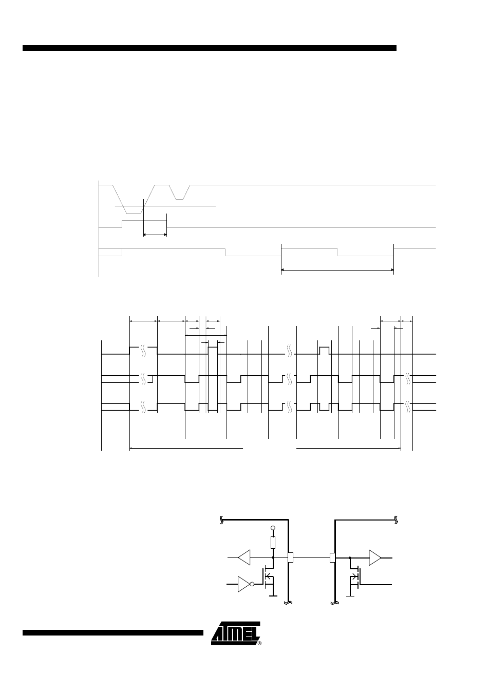
Figure 19. Generation of the Power-on Reset
Figure 20. Timing of the Register Programming
Programming the
Configuration Register
The configuration registers are programmed serially via the bi-directional data line
according to Figure 20 and Figure 21.
Figure 21. One-wire Connection to a Microcontroller
V
S
POR
DATA (U3741BM)
X
1/f
RM
V
ThReset
t
Rst
Out1
(microcontroller)
DATA (U3741BM)
Serial bi-directional
data line
X
Bit 1
("0")
Bit 2
("1")
Bit 13
("0")
Bit 14
("1")
X
t1
t2
t3
t4
t5
t6
t8
t7
X
X
T
Sleep
Programming Frame
(Start bit)
(Register select)
(Poll8)
(Poll8R)
Receiver
on
Startup
mode
t9
Internal pull-up
resistor
Bi-directional
data line
DATA
I/O
U3741BM
microcontroller
DATA (U3741BM)
Out 1 (µC)