Bit check mode, Configuring the bit check, U3741bm – Rainbow Electronics U3741BM User Manual
Page 13
13
U3741BM
4662B–RKE–10/04
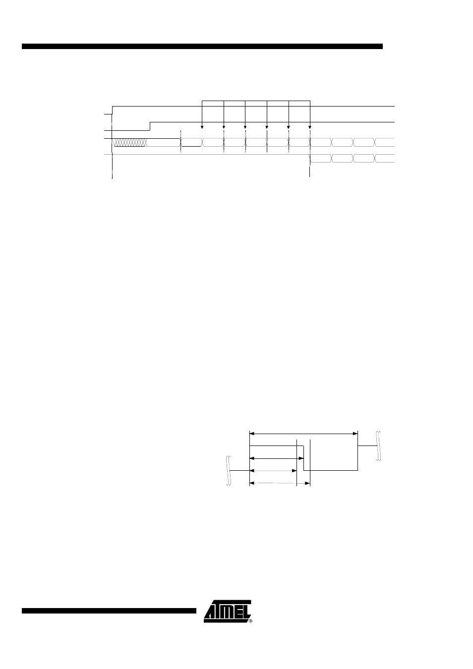
Figure 9. Timing Diagram for a Completely Successful Bit Check
Bit Check Mode
In bit check mode, the incoming data stream is examined to distinguish between a valid
signal from a corresponding transmitter and signals due to noise. This is done by subse-
quent time frame checks where the distances between 2 signal edges are continuously
compared to a programmable time window. The maximum count of this edge-to-edge
test, before the receiver switches to receiving, mode is also programmable.
Configuring the Bit Check
Assuming a modulation scheme that contains 2 edges per bit, two time frame checks
are verifying one bit. This is valid for Manchester, Bi-phase and most other modulation
schemes. The maximum count of bits to be checked can be set to 0, 3, 6 or 9 bits via the
variable N
Bitcheck
in the OPMODE register. This implies 0, 6, 12 and 18 edge-to-edge
checks respectively. If N
Bitcheck
is set to a higher value, the receiver is less likely to
switch to the receiving mode due to noise. In the presence of a valid transmitter signal,
the bit check takes less time if N
Bitcheck
is set to a lower value. In polling mode, the bit
check time is not dependent on N
Bitcheck
. Figure 9 shows an example where 3 bits are
tested successfully and the data signal is transferred to pin DATA.
According to Figure 10, the time window for the bit check is defined by two separate
time limits. If the edge-to-edge time t
ee
is in between the lower bit check limit T
Lim_min
and
the upper bit check limit T
Lim_max
, the check will be continued. If t
ee
is smaller than
T
Lim_min
or t
ee
exceeds T
Lim_max
, the bit check will be terminated and the receiver
switches to sleep mode.
Figure 10. Valid Time Window for Bit Check
For best noise immunity it is recommended to use a low span between T
Lim_min
and
T
Lim_max
. This is achieved using a fixed frequency at a 50% duty cycle for the transmitter
preburst. A ‘11111...’ or a ‘10101...’ sequence in Manchester or Bi-phase is a good
choice in this regard. A good compromise between receiver sensitivity and susceptibility
to noise is a time window of ±25% regarding the expected edge-to-edge time t
ee
. Using
preburst patterns that contain various edge-to-edge time periods, the bit check limits
must be programmed according to the required span.
Bit check
Enable IC
DATA
1/2 Bit
Polling mode
Number of Checked Bits: 3
Bit check ok
1/2 Bit
1/2 Bit
1/2 Bit
1/2 Bit
1/2 Bit
Receiving mode
Dem_out
Dem_out
t
ee
T
lim_min
1/f
Sig
T
lim_max