Duration of the bit check, Receiving mode, Digital signal processing – Rainbow Electronics U3741BM User Manual
Page 15: U3741bm
15
U3741BM
4662B–RKE–10/04
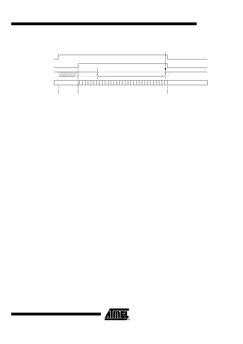
Figure 13. Timing Diagram for Failed Bit Check (Condition: CV_Lim
≥
Lim_max)
Duration of the Bit Check
If no transmitter signal is present during the bit check, the output of the ASK/FSK
demodulator delivers random signals. The bit check is a statistical process and T
Bitcheck
varies for each check. Therefore, an average value for T
Bitcheck
is given in “Electrical
Characteristics”. T
Bitcheck
depends on the selected baud rate range and on T
Clk
. A higher
baudrate range causes a lower value for T
Bitcheck
resulting in lower current consumption
in polling mode.
In the presence of a valid transmitter signal, T
Bitcheck
is dependant on the frequency of
that signal, f
Sig
and the count of the checked bits, N
Bitcheck
. A higher value for N
Bitcheck
thereby results in a longer period for T
Bitcheck
requiring a higher value for the transmitter
preburst T
Preburst
.
Receiving Mode
If the bit check has been successful for all bits specified by N
Bitcheck
, the receiver
switches to receiving mode. According to Figure 9 on page 13, the internal data signal is
switched to pin DATA in that case. A connected microcontroller can be woken up by the
negative edge at pin DATA. The receiver stays in that condition until it is switched back
to polling mode explicitly.
Digital Signal Processing
The data from the ASK/FSK demodulator (Dem_out) is digitally processed in different
ways and as a result converted into the output signal data. This processing depends on
the selected baud rate range (BR_Range). Figure 14 on page 16 illustrates how
Dem_out is synchronized by the extended clock cycle T
XClk
. This clock is also used for
the bit check counter. Data can change its state only after T
XClk
elapsed. The
edge-to-edge time period t
ee
of the Data signal as a result is always an integral multiple
of T
XClk
.
The minimum time period between two edges of the data signal is limited to
t
ee
≥
T
DATA_min
. This implies an efficient suppression of spikes at the DATA output. At the
same time, it limits the maximum frequency of edges at DATA. This eases the interrupt
handling of a connected microcontroller. T
DATA_min
is to some extent affected by the pre-
ceding edge-to-edge time interval t
ee
as illustrated in Figure 15. If t
ee
is in between the
s p e c i fi e d b i t c h e c k l i m i ts , t he f o l l ow i n g l e v e l i s f ro z e n f o r th e t i me p e ri o d
T
DATA_min
= tmin1, in case of t
ee
being outside that bit check limits T
DATA_min
= tmin2 is the
relevant stable time period.
The maximum time period for DATA to be low is limited to T
DATA_L_max
. This function
ensures a finite response time during programming or switching off the receiver via pin
DATA. T
DATA_L_max
is thereby longer than the maximum time period indicated by the
transmitter data stream. Figure 16 gives an example where Dem_out remains low after
the receiver has switched to receiving mode.
Bit check
Enable IC
Bit check
Counter
0
2 3 4 5 6
2
4 5
1
7
3
6 7 8 9
1112
10
1/2 Bit
Startup Mode
20
(Lim_min = 14, Lim_max = 24)
Sleep Mode
Bit check failed (CV_Lim = Lim_max)
13141516171819
21222324
0
1
Dem_out
Bit check Mode