Detailed description, Table 1. register address map – Rainbow Electronics MAX9135 User Manual
Page 9
MAX9132/MAX9134/MAX9135
Programmable, High-Speed, Multiple
Input/Output LVDS Crossbar Switches
_______________________________________________________________________________________
9
Detailed Description
The MAX9132/MAX9134/MAX9135 high-speed, multi-
ple-port, low-voltage differential signaling (LVDS)
crossbar switches are specially designed for digital
video and camera signal transmission. These switches
have a wide bandwidth, supporting data rates up to
840Mbps. This allows the use of MAX9132/MAX9134/
MAX9135 with LVDS serializers/deserializers (SerDes)
to create a complete video or camera network. The
MAX9132 has three input ports and two output ports,
the MAX9134 has three input ports and four output
ports, and the MAX9135 has four input ports and three
output ports. The video or camera signal can go
through the switch from an input port to one or multiple
output ports.
The MAX9132/MAX9134/MAX9135 switch routing is
programmable through either an I
2
C interface or a
Local Interconnect Network (LIN) serial interface. AS0
and AS1 set the slave addresses for either of these
modes, allowing several devices on a bus simultane-
ously. In addition, the MAX9134/MAX9135 provide
3-level pins S[5:0] to set switch routing and the initial
conditions for I
2
C mode. To improve the signal integrity,
all the LVDS outputs feature selectable preemphasis.
Initial Power-Up
On power-up, all control registers have a value of 0x00.
For the MAX9134/MAX9135, leaving S[5:0] unconnect-
ed, allows control through the LIN interface with all out-
puts deactivated. Otherwise, the switch runs in
pin-control mode with S[5:0] controlling the switch rout-
ing. The I
2
C is also active while the device is in pin-
control mode. Successful routing through I
2
C overrides
the pin settings. For more details, see the
I
2
C Interface
section. For the MAX9132, the FS input determines
which interface is active.
Register Description
There are four 1-byte control registers in the
MAX9132/MAX9134/MAX9135. These registers control
the routing of the switch. Table 1 describes the register
map for both I
2
C and LIN. When the MAX9132/
MAX9134/MAX9135 operate in LIN mode, register 0x00
acts as an error flag register. Its function is described
in detail in Table 5. In either I
2
C or LIN mode, the con-
trol registers (0x01, 0x02) program the MAX9132/
MAX9134/MAX9135 switch routing control. In addition,
these registers can individually activate and deactivate
preemphasis for each output port. Table 2a describes
the routing for the MAX9132/MAX9134 and Table 2b for
the MAX9135. For I
2
C programming, register 0xFF con-
trols the activation of routing.
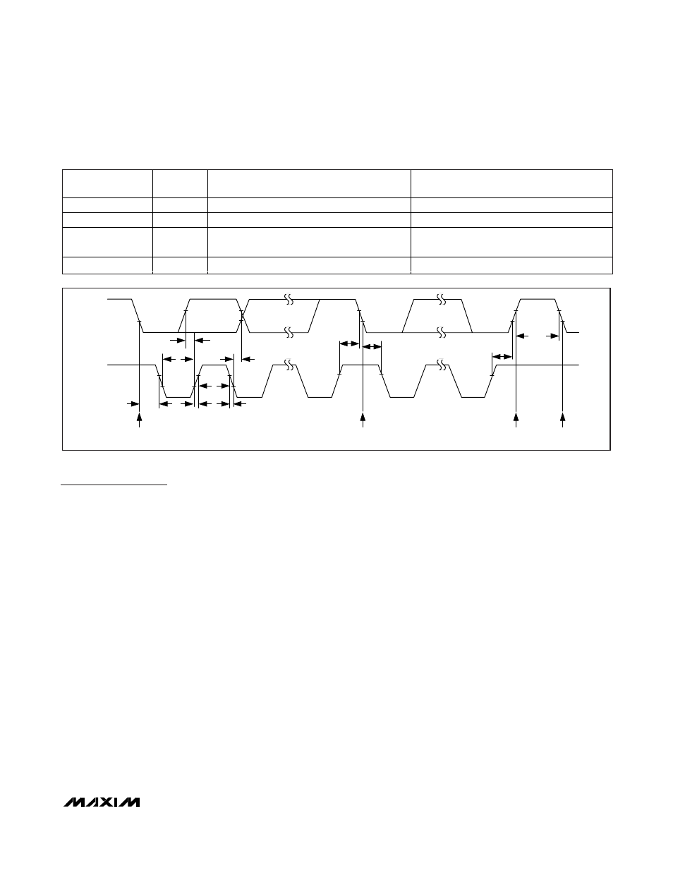
SDA
SCL
t
HD:STA
t
LOW
t
HIGH
t
R
t
F
t
SU:DAT
t
SU:STA
t
SU:STO
t
BUF
t
HD:STA
t
HD:DAT
START
CONDITION
STOP
CONDITION
START
CONDITION
REPEATED
START CONDITION
Figure 1. I
2
C Serial-Interface Timing Details
REGISTER
ADDRESS (HEX)
READ/
WRITE
LIN INTERFACE DESCRIPTION
I
2
C DESCRIPTION
0x00
R
LIN Status Register
Reserved
0x01
R/W
Switch Control Register 1
Switch Control Register 1
0x02
R/W
Switch Control Register 2 (MAX9134/MAX9135
only)
Switch Control Register 2 (MAX9134/MAX9135
only)
0xFF
W
Reserved
Route Activation Register
Table 1. Register Address Map