Pin description (continued) – Rainbow Electronics MAX9135 User Manual
Page 7
MAX9132/MAX9134/MAX9135
Programmable, High-Speed, Multiple
Input/Output LVDS Crossbar Switches
_______________________________________________________________________________________
7
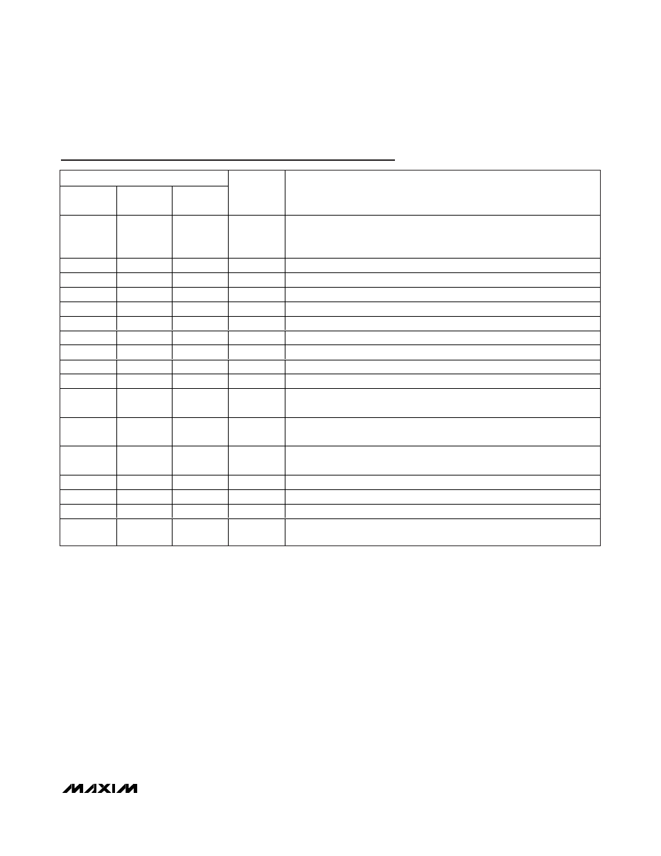
PIN
MAX9132
TSSOP
MAX9134
TQFP
MAX9135
TQFP
NAME
FUNCTION
12
14
15
AS1/NSLP
3-Level I
2
C Address Selection 1 Input (in I
2
C Mode, Table 3). In LIN bus
mode, it becomes an NSLP output, the sleep mode activation pin (active
low) to the LIN bus driver.
13
16, 25
19, 24
LVDSGND
LVDS Ground
—
17
—
DOUT3-
Port 3 Negative Output
—
18
—
DOUT3+
Port 3 Positive Output
—
19
17
DOUT2-
Port 2 Negative Output
—
20
18
DOUT2+
Port 2 Positive Output
14
21
20
DOUT1-
Port 1 Negative Output
15
22
21
DOUT1+
Port 1 Positive Output
16
23
22
DOUT0-
Port 0 Negative Output
17
24
23
DOUT0+
Port 0 Positive Output
18
15, 26
16, 25
LVDSVDD
LVDS Supply Input. Bypass LVDSVDD to LVDSGND with 0.1µF and 0.01µF
capacitors as close as possible to the device.
19
27
26
SDA/TXD
I
2
C Data Link Input/LIN Tx Output. SDA/TXD becomes SDA when in I
2
C
mode and TXD when in LIN mode.
20
28
27
SCL/RXD
I
2
C Clock/LIN Rx Input. SCL/RXD becomes SCL when in I
2
C mode and RXD
when in LIN mode.
—
29
28
S5
Routing Selection 5 Input. See Tables 6a and 6b.
—
30
29
S4
Routing Selection 4 Input. See Tables 6a and 6b.
—
—
32
DGND
Digital Ground
—
—
—
EP
Exposed Pad. Internally connected to GND. Connect to a large ground
plane to maximize thermal performance.
Pin Description (continued)