Rainbow Electronics MAX9135 User Manual
Page 14
MAX9132/MAX9134/MAX9135
Interface Selection Using S[5:0]
(MAX9134/MAX9135)
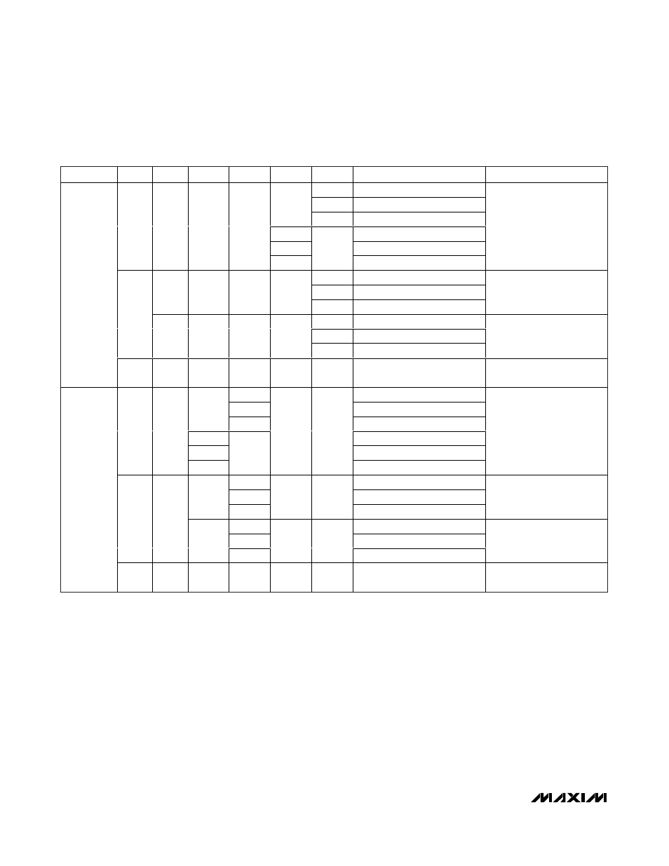
S[5:0] determine which interface controls the
MAX9134/MAX9135. Leave S[5:0] unconnected or set
to a midlevel state to enable the LIN interface. Other
settings to S[5:0] set the switch routing according to
Tables 6a (MAX9134) and 6b (MAX9135). The I
2
C inter-
face is active when the MAX9132/MAX9134/MAX9135
are not in LIN interface mode. Writing to an I
2
C register
overrides the S[5:0] settings.
Interface Selection Using FS
(MAX9132 Only)
The FS input selects the interface for the MAX9132. Set
FS high for LIN interface control and FS low for I
2
C
interface. The MAX9132 powers up with all LVDS out-
puts unconnected for either mode.
Interfacing the
MAX9132/MAX9134/MAX9135
to the LIN Bus
The MAX9132/MAX9134/MAX9135 interface to the LIN
bus through the MAX13020 LIN transceivers. This
device translates the +12V to +42V LIN bus signal down
Programmable, High-Speed, Multiple
Input/Output LVDS Crossbar Switches
14
______________________________________________________________________________________
PORT
S5
S4
S3
S2
S1
S0
CONNECTION
DESCRIPTION
0
DOUT0 connected to DIN0
Open
DOUT0 connected to DIN1
X
1
DOUT0 connected to DIN2
0
DOUT1 connected to DIN0
Open
DOUT1 connected to DIN1
0
X
X
X
1
X
DOUT1 connected to DIN2
Both DOUT0 and DOUT1
outputs are on
0
DOUT0 connected to DIN0
Open
DOUT0 connected to DIN1
X
X
X
0
1
DOUT0 connected to DIN2
DOUT1 is not connected,
DOUT0 is on
0
DOUT1 connected to DIN0
Open
DOUT1 connected to DIN1
1
X
X
X
Open
1
DOUT1 connected to DIN2
DOUT0 is not connected,
DOUT1 is on
DOUT0,
DOUT1
1
X
X
X
1
X
DOUT0 and DOUT1
in high impedance
Both DOUT0 and DOUT1
are not connected
0
DOUT2 connected to DIN0
Open
DOUT2 connected to DIN1
X
1
DOUT2 connected to DIN2
0
DOUT3 connected to DIN0
Open
DOUT3 connected to DIN1
X
0
1
X
X
X
DOUT3 connected to DIN2
Both DOUT2 and DOUT3
outputs are on
0
DOUT2 connected to DIN0
Open
DOUT2 connected to DIN1
0
1
X
X
DOUT2 connected to DIN2
DOUT3 is not connected,
DOUT2 is on
0
DOUT3 connected to DIN0
Open
DOUT3 connected to DIN1
X
1
Open
1
X
X
DOUT3 connected to DIN2
DOUT2 is not connected,
DOUT3 is on
DOUT2,
DOUT3
X
1
1
X
X
X
DOUT2 and DOUT3
in high impedance
Both DOUT2 and DOUT3
are not connected
Table 6a. Switch Routing Control Pin Setting for the MAX9134
X = Don’t care.